M41T11M6F STMicroelectronics, M41T11M6F Datasheet
M41T11M6F
Specifications of M41T11M6F
Available stocks


Related parts for M41T11M6F


M41T11M6F Summary of contents
Page 1
Features ■ Counters for seconds, minutes, hours, day, date, month, years and century ■ 32 KHz crystal oscillator integrating load capacitance (12.5 pF) providing exceptional oscillator stability and high crystal series resistance operation 2 ■ Serial interface supports I protocol) ...
Page 2
Contents Contents 1 Description . . . . . . . . . . . . . . . . . . . . . . . . . . . . . . . . . . . . ...
Page 3
M41T11 List of tables Table 1. Signal names . . . . . . . . . . . . . . . . . . . . . . . . . . . . . . . . ...
Page 4
List of figures List of figures Figure 1. Logic diagram . . . . . . . . . . . . . . . . . . . . . . . . . . . . . . ...
Page 5
M41T11 1 Description The M41T11is a low-power serial real time clock with 56 bytes of NVRAM. A built-in 32.768 kHz oscillator (external crystal controlled) and the first 8 bytes of the RAM are used for the clock/calendar function and are ...
Page 6
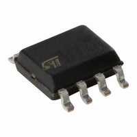
Description Table 1. Signal names OSCI OCSO FT/OUT SDA SCL V BAT Figure 2. 8-pin SOIC connections Figure 3. 28-pin SOIC connections 6/30 Oscillator input Oscillator output Frequency test/output driver (open drain) Serial data address input/output ...
Page 7
M41T11 Figure 4. Block diagram OSCI OSCILLATOR 32.768 kHz OSCO FT/OUT VOLTAGE V CC SENSE and V SS SWITCH V BAT CIRCUITRY SCL SERIAL BUS INTERFACE SDA 1 Hz SECONDS DIVIDER CENTURY/HOURS CONTROL LOGIC ADDRESS REGISTER Description MINUTES DAY DATE ...
Page 8
Operation 2 Operation The M41T11 clock operates as a slave device on the serial bus. Access is obtained by implementing a start condition followed by the correct slave address (D0h). The 64 bytes contained in the device can then be ...
Page 9
M41T11 2.1.3 Stop data transfer A change in the state of the data line, from low to high, while the clock is high, defines the STOP condition. 2.1.4 Data valid The state of the data line represents valid data when ...
Page 10
Operation Figure 6. Acknowledgement sequence START SCLK FROM MASTER DATA OUTPUT BY TRANSMITTER DATA OUTPUT BY RECEIVER Figure 7. Bus timing requirements sequence SDA tBUF SCL STOP and S = START 10/ MSB ...
Page 11
M41T11 Table 2. AC characteristics Symbol f SCL clock frequency SCL t Clock low period LOW t Clock high period HIGH t SDA and SCL rise time R t SDA and SCL fall time F START condition hold time t ...
Page 12
Operation Figure 8. Slave address location START Figure 9. Read mode sequence BUS ACTIVITY: MASTER SDA LINE S BUS ACTIVITY: SLAVE ADDRESS DATA n+X Figure 10. Alternate read mode sequence BUS ACTIVITY: MASTER SDA LINE S BUS ACTIVITY: SLAVE ADDRESS ...
Page 13
M41T11 2.3 Write mode In this mode the master transmitter transmits to the M41T11 slave receiver. Bus protocol is shown in Figure 11. Following the START condition and slave address, a logic '0' (R placed on the ...
Page 14
Clock operation 3 Clock operation The eight byte clock register (see and time from the clock binary coded decimal format. Seconds, minutes, and hours are contained within the first three registers. Bits D6 and D7 of clock register ...
Page 15
M41T11 Table 3. Register map Address (2) 2 CEB OUT 1. Keys SIGN bit FT = FREQUENCY TEST bit ST = STOP bit OUT = ...
Page 16
Clock operation adjustment per calibration step in the calibration register. Assuming that the oscillator is in fact running at exactly 32,768 Hz, each of the 31 increments in the calibration byte would represent +10.7 or –5.35 seconds per month which ...
Page 17
M41T11 Figure 12. Crystal accuracy across temperature Frequency (ppm –20 –40 –60 –80 –100 –120 –140 –160 –40 –30 –20 Figure 13. Clock calibration NORMAL POSITIVE CALIBRATION NEGATIVE CALIBRATION – ...
Page 18
... These are stress ratings only and operation of the device at these or any other conditions above those indicated in the operating sections of this specification is not implied. Exposure to absolute maximum rating conditions for extended periods may affect device reliability. Refer also to the STMicroelectronics SURE Program and other relevant quality documents. Table 4. ...
Page 19
M41T11 5 DC and AC parameters This section summarizes the operating and measurement conditions, as well as the DC and AC characteristics of the device. The parameters in the following DC and AC characteristic tables are derived from tests performed ...
Page 20
... C Load capacitance L 1. These values are externally supplied if using the SO8 package. STMicroelectronics recommends the KDS DT-38: 1TA/1TC252E127, Tuning Fork Type (thru-hole) or the DMX-26S: 1TJS125FH2A212, (SMD) quartz crystal for industrial temperature operations. KDS can be contacted at kouhou@kdsj.co.jp or http://www.kdsj.co.jp for further information on this crystal type. ...
Page 21
M41T11 Figure 15. Power down/up mode AC waveforms tPD SDA SCL Table 9. Power down/up AC characteristics Symbol t SCL and SDA SCL and SDA at V REC 1. Valid for ambient ...
Page 22
Package mechanical data 6 Package mechanical data In order to meet environmental requirements, ST offers these devices in different grades of ® ECOPACK packages, depending on their level of environmental compliance. ECOPACK specifications, grade definitions and product status are available ...
Page 23
M41T11 Figure 16. SO8 – 8-lead plastic small outline package outline A2 1. Drawing is not to scale. Table 11. SO8 – 8-lead plastic small outline (150 mils body width) package mechanical data Symbol ccc ...
Page 24
Package mechanical data Figure 17. SOH28 – 28-lead plastic small outline, battery SNAPHAT outline 1. Drawing is not to scale. Table 12. SOH28 – 28-lead plastic small outline, battery SNAPHAT mechanical data Symb ...
Page 25
M41T11 Figure 18. SH – 4-pin SNAPHAT outline 1. Drawing is not to scale. Table 13. SH – 4-pin SNAPHAT mechanical data Symb ® housing for 48 mAh battery & ...
Page 26
Package mechanical data Figure 19. SH – 4-pin SNAPHAT outline 1. Drawing is not to scale. Table 14. SH – 4-pin SNAPHAT mech. data Symb 26/30 ® housing for 120 ...
Page 27
M41T11 7 Part numbering Table 15. Ordering information scheme Example: Device type M41T Supply voltage 2 Package M = SO8 (150 mil width) ( SOH28 Temperature range 6 = –40 ...
Page 28
Environmental information 8 Environmental information Figure 20. Recycling symbols This product contains a non-rechargeable lithium (lithium carbon monofluoride chemistry) button cell battery fully encapsulated in the final product. Recycle or dispose of batteries in accordance with the battery manufacturer's instructions ...
Page 29
M41T11 9 Revision history Table 17. Revision history Date Revision Mar-1999 23-Dec-1999 25-Jul-2000 12-Dec-2000 24-Jan-2001 27-Feb-2001 17-Jul-2001 27-Nov-2001 21-Jan-2002 01-May-2002 03-Jul-2002 07-Nov-2002 15-Jun-2004 14-Dec-2004 22-Aug-2006 03-Oct-2007 02-May-2008 08-Jan-2009 1 First issue 1.1 SOH28 package added 1.2 Crystal electrical characteristics: R ...
Page 30
... Information in this document is provided solely in connection with ST products. STMicroelectronics NV and its subsidiaries (“ST”) reserve the right to make changes, corrections, modifications or improvements, to this document, and the products and services described herein at any time, without notice. All ST products are sold pursuant to ST’s terms and conditions of sale. ...