STEVAL-ISA029V1 STMicroelectronics, STEVAL-ISA029V1 Datasheet - Page 24
STEVAL-ISA029V1
Manufacturer Part Number
STEVAL-ISA029V1
Description
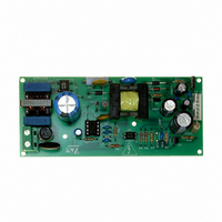
BOARD EVAL BASED ON VIPER53-E
Manufacturer
STMicroelectronics
Series
VIPER™r
Type
MOSFET & Power Driverr
Specifications of STEVAL-ISA029V1
Design Resources
STEVAL-ISA029V1 Gerber Files STEVAL-ISA029V1 Schematic STEVAL-ISA029V1 Bill of Material
Main Purpose
AC/DC, Primary Side
Outputs And Type
3, Isolated
Power - Output
13W
Voltage - Output
12V, 3.3V, -24V
Current - Output
1A, 100mA, 40mA
Voltage - Input
85 ~ 300VAC
Regulator Topology
Flyback
Frequency - Switching
60kHz
Board Type
Fully Populated
Utilized Ic / Part
VIPer53
Input Voltage
85 V to 300 V
Output Voltage
12 V
Product
Power Management Modules
Silicon Manufacturer
ST Micro
Silicon Core Number
VIPer53-E
Kit Application Type
Power Management
Application Sub Type
Power Supply
Kit Contents
Board
Rohs Compliant
No
Lead Free Status / RoHS Status
Lead free / RoHS Compliant
For Use With/related Products
VIPer53-E
Other names
497-6458
STEVAL-ISA029V1
STEVAL-ISA029V1


Short-circuit and overload protection
10
24/36
Short-circuit and overload protection
A V
V
When reaching typically V
stops switching. This state is latched because of to the regulation loop which maintains the
COMP pin voltage above the V
more energy from the auxiliary winding, its voltage drops down until it reaches V
the device is reset, recharging the V
drops below the V
resumes switching immediately.
The device enters an endless restart sequence if the overload or short circuit condition is
maintained. The restart duty cycle D
to restart, thus delivering its full power capability to the output. In order to keep the whole
converter in a safe state during this event, D
compromising the real start-up of the converter. A typical value of about 10% is generally
sufficient. For this purpose, both V
following conditions:
Equation 6
Equation 7
Refer to the previous start-up section for the definition of tss, and C
checked against the limit given in this section. The maximum value of the two calculus will
be adopted.
All this behavior can be observed on
of the drain current Id for V
is the drain current to take into account for design purposes. Since I
maximum value for which the overload protection is not triggered, it defines the power
capability of the power supply.
COMP
COMPovl
goes above this level, the capacitor connected on the TOVL pin begins to charge.
threshold of about 4.35V has been implemented on the COMP pin. When
COMPovl
C
OVLth
VDD
threshold for any reason during the VDD drop, the device
COMP
COMPovl
(4V), the internal MOSFET driver is disabled and the device
8
= V
DD
C
10
RST
OVL
DD
COMPovl
Figure 8 on page
4
and TOVL capacitors can be used to satisfy the
threshold. Since the V
capacitor for a new restart cycle. Note: If VCOMP
is defined as the time ratio for which the device tries
12.5
------------- - 1
D
RST
1
RST
is shown. The corresponding parameter I
–
10
must be kept as low as possible, without
–
6
C
-------------------------------------- -
10. In
tss
OVL
V
DDhyst
Figure 10 on page 11
I
DD
DDch2
pin does not receive any
VDD
Dmax
must also be
represents the
VIPer53 - E
DDoff
the value
and
Dmax
Related parts for STEVAL-ISA029V1
Image
Part Number
Description
Manufacturer
Datasheet
Request
R

Part Number:
Description:
BOARD RGB CTR ST7,STP08C596MTR
Manufacturer:
STMicroelectronics
Datasheet:

Part Number:
Description:
Power Management IC Development Tools Full Speed USB to RS232 Bridge Demo
Manufacturer:
STMicroelectronics
Datasheet:
Part Number:
Description:
Power Management IC Development Tools 2.5W solar eval BRD USB SPV1040 LD39050
Manufacturer:
STMicroelectronics
Datasheet:

Part Number:
Description:
BOARD EVAL FOR MEMS SENSORS
Manufacturer:
STMicroelectronics
Datasheet:

Part Number:
Description:
KIT DEV STARTER ST10F276Z5
Manufacturer:
STMicroelectronics
Datasheet:

Part Number:
Description:
BOARD EVAL HDMI $ VIDEO SWITCH
Manufacturer:
STMicroelectronics
Datasheet:

Part Number:
Description:
BOARD DEMO ACCELEROMETER DIL24
Manufacturer:
STMicroelectronics
Datasheet:

Part Number:
Description:
BOARD STLM75/STDS75/ST72F651
Manufacturer:
STMicroelectronics
Datasheet:

Part Number:
Description:
EVAL BOARD 3AXIS MEMS ACCELLRMTR
Manufacturer:
STMicroelectronics
Datasheet:

Part Number:
Description:
BOARD EVAL 8BIT MICRO + TDE1708
Manufacturer:
STMicroelectronics
Datasheet:
Part Number:
Description:
STMicroelectronics [RIPPLE-CARRY BINARY COUNTER/DIVIDERS]
Manufacturer:
STMicroelectronics
Datasheet:
Part Number:
Description:
STMicroelectronics [LIQUID-CRYSTAL DISPLAY DRIVERS]
Manufacturer:
STMicroelectronics
Datasheet:
Part Number:
Description:
BOARD EVAL FOR MEMS SENSORS
Manufacturer:
STMicroelectronics
Datasheet: