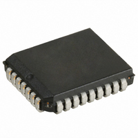
CY7C4261V-10JC Cypress Semiconductor Corp, CY7C4261V-10JC Datasheet

CY7C4261V-10JC
Specifications of CY7C4261V-10JC
Available stocks
Related parts for CY7C4261V-10JC
CY7C4261V-10JC Summary of contents
Page 1
... High-speed, low-power, first-in first-out (FIFO) memories • 16K × 9 (CY7C4261V) • 32K × 9 (CY7C4271V) • 64K × 9 (CY7C4281V) • 128K × 9 (CY7C4291V) • 0.35-micron CMOS for optimum speed/power • ...
Page 2
... Resets device to empty condition. A reset is required before an initial read or write operation after power-up. I When OE is LOW, the FIFO’s data outputs drive the bus to which they are connected HIGH, the FIFO’s outputs are in High Z (high-impedance) state. CY7C4261V/CY7C4271V CY7C4281V/CY7C4291V 7C4261/71/81/91V-25 66.7 40 ...
Page 3
... WEN2/LD and WEN1 are LOW. The fifth LOW-to-HIGH transition of WCLK while WEN2/LD and WEN1 are LOW writes data to the empty LSB register again. Figure 1 shows before ENS the registers sizes and default values for the various device types. 0–8 CY7C4261V/CY7C4271V CY7C4281V/CY7C4291V outputs 0-8 outputs 0-8 Page ...
Page 4
... PAF. PAE is synchronized to the LOW-to-HIGH transition of WCLK by one flip-flop and is set LOW when the number of unread words in the FIFO is greater than or equal to CY7C4261V (16k – m), CY7C4271V (32k – m), CY7C4281V (64k - m) and CY7C4291V (128k – m). PAF is set HIGH by the LOW-to-HIGH transition of WCLK when the number of available memory locations is greater than m ...
Page 5
... The Empty Flag (EF) will go LOW when the device is empty. Read operations are inhibited whenever EF is LOW, regardless of the state of REN1 and REN2 synchronized to RCLK, i.e exclusively updated by each rising edge of RCLK. RESET (RS) 9 CY7C4261V CY7C4271V CY7C4281V CY7C4291V Read Enable 2 (REN2) Used in a Width-Expansion Configuration CY7C4261V/CY7C4271V CY7C4281V/CY7C4291V CY7C4291V FF PAF [ (m+1)) ...
Page 6
... V < Com’l 25 Ind Com’l 4 Ind Description Test Conditions MHz 3.3V CC [8, 9] 3.0V R2=510 GND 2.0V . CY7C4261V/CY7C4271V CY7C4281V/CY7C4291V Ambient Temperature 0°C to +70°C 40°C to +85°C 7C4261/71/81/91V- 7C4261/71/81/91V Min. Max. Min. 2.4 2.4 0.4 2 0.5 0.8 0.5 10 ...
Page 7
... Pulse widths less than minimum values are not allowed. 11. Values guaranteed by design, not currently tested. Document #: 38-06013 Rev. *A (-10) (continued) CC/2 3.0V GND 3 ns 7C4261/71/81/91V- 10 Min. Max. 100 4.5 4.5 3 [11 [11 CY7C4261V/CY7C4271V CY7C4281V/CY7C4291V All Input Pulses 90% 90% 10% 10 7C4261/71/81/91V- 7C4261/71/81/91V Min. Max. Min. Max. 66 ...
Page 8
... CLKL t ENH NO OPERATION t REF [13] t SKEW1 , then FF may not change state until the next WCLK rising edge. SKEW1 , then EF may not change state until the next RCLK rising edge. SKEW2 CY7C4261V/CY7C4271V CY7C4281V/CY7C4291V ENH NO OPERATION NO OPERATION t WFF t REF VALID DATA t OHZ Page ...
Page 9
... Holding WEN2/LD HIGH during reset will make the pin act as a second enable pin. Holding WEN2/LD LOW during reset will make the pin act as a load enable for the programmable flag offset registers. Document #: 38-06013 Rev RSS t RSS t RSS t RSF t RSF t RSF CY7C4261V/CY7C4271V CY7C4281V/CY7C4291V t RSR t RSR t RSR [15 OE=0 Page ...
Page 10
... The Latency Timing applies only at the Empty Boundary (EF = LOW). 18. The first word is available the cycle after EF goes HIGH, always. Document #: 38-06013 Rev [17] t FRL t SKEW1 t REF t OLZ t OE (maximum When t < minimum specification, t CLK SKEW2 SKEW1 CY7C4261V/CY7C4271V CY7C4281V/CY7C4291V [18 (maximum) = either 2 FRL CLK SKEW1 Page ...
Page 11
... ENS WEN1 t t ENS ENH WEN2 (if applicable) t FRL RCLK t SKEW1 EF REN1, REN2 LOW OE DATA IN OUTPUT REGISTER Q – Document #: 38-06013 Rev [17 REF REF t A CY7C4261V/CY7C4271V CY7C4281V/CY7C4291V DATA WRITE 2 t ENH t ENS t t ENH ENS [17] t FRL t t REF SKEW1 DATA READ Page ...
Page 12
... Document #: 38-06013 Rev DATA WRITE t WFF t ENH t A DATA READ t CLKL t t ENS ENH Note ENS ENH [19] t PAE CY7C4261V/CY7C4271V CY7C4281V/CY7C4291V NO WRITE [12] t SKEW1 t t WFF WFF t ENH t ENS t A NEXT DATA READ WORDS Note21 IN FIFO ENS ENS ENH DATA WRITE ...
Page 13
... If a write is performed on this rising edge of the write clock, there will be Full 23. PAF offset = m. 24. 16K m words for CY7C4261V, 32K – m words for CY7C4271V, 64K 25 the minimum time between a rising RCLK edge and a rising WCLK edge for PAF to change during that clock cycle. If the time between the rising edge of RCLK ...
Page 14
... CLKH RCLK t ENS WEN2/LD t ENS REN1, REN2 Q – Ordering Information 16Kx9 Low-voltage Deep Sync FIFO Speed (ns) Ordering Code 10 CY7C4261V-10JC 15 CY7C4261V-15JC CY7C4261V-15JI 25 CY7C4261V-25JC 32Kx9 Low-voltage Deep Sync FIFO Speed (ns) Ordering Code 10 CY7C4271V-10JC 15 CY7C4271V-15JC CY7C4271V-15JI 25 CY7C4271V-25JC 64kx9 Low-voltage Deep Sync FIFO Speed (ns) ...
Page 15
... The inclusion of Cypress Semiconductor products in life-support systems application implies that the manufacturer assumes all risk of such use and in doing so indemnifies Cypress Semiconductor against all charges. 32-Lead Plastic Leaded Chip Carrier J65 CY7C4261V/CY7C4271V CY7C4281V/CY7C4291V 51-85002-*B ...
Page 16
... Document History Page Document Title: CY7C4261V/CY7C4271V/CY7C4281V/CY7C4291V 16K/32K/64K/128K/X9 Low-Voltage Deep Sync FIFO Document Number: 38-06013 Orig. of REV. ECN NO. Issue Date Change ** 106474 09/15/01 *A 127858 09/04/03 Document #: 38-06013 Rev. *A SZV Changed Spec number from 38-00656 to 38-06013 FSG Changed SKEW2 SKEW1 Fixed flag timing diagram in Switching Waveforms section ...


