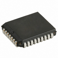
CY7C4261-15JXC Cypress Semiconductor Corp, CY7C4261-15JXC Datasheet - Page 8

CY7C4261-15JXC
Manufacturer Part Number
CY7C4261-15JXC
Description
IC DEEP SYNC FIFO 16KX9 32-PLCC
Manufacturer
Cypress Semiconductor Corp
Series
CY7Cr
Specifications of CY7C4261-15JXC
Function
Synchronous
Memory Size
144K (16K x 9)
Data Rate
100MHz
Access Time
10ns
Voltage - Supply
3.3V
Operating Temperature
-40°C ~ 85°C
Mounting Type
Surface Mount
Package / Case
32-PLCC
Configuration
Dual
Density
144Kb
Access Time (max)
10ns
Word Size
9b
Organization
16Kx9
Sync/async
Synchronous
Expandable
Yes
Bus Direction
Uni-Directional
Clock Freq (max)
66.7MHz
Operating Supply Voltage (typ)
5V
Operating Supply Voltage (min)
4.5V
Operating Supply Voltage (max)
5.5V
Supply Current
35mA
Operating Temp Range
0C to 70C
Operating Temperature Classification
Commercial
Mounting
Surface Mount
Pin Count
32
Lead Free Status / RoHS Status
Lead free / RoHS Compliant
Available stocks
Company
Part Number
Manufacturer
Quantity
Price
Company:
Part Number:
CY7C4261-15JXC
Manufacturer:
Cypress Semiconductor Corp
Quantity:
10 000
Company:
Part Number:
CY7C4261-15JXCT
Manufacturer:
Cypress Semiconductor Corp
Quantity:
10 000
Switching Characteristics
Over the Operating Range
Notes
Document #: 38-06015 Rev. *D
t
t
t
t
t
t
t
t
t
t
t
t
t
t
t
t
t
t
t
t
t
t
Parameter
10. 5CL = 30 pF for all AC parameters except for t
11. 5CL = 5 pF for t
12. Pulse widths less than minimum values are not allowed.
13. Values guaranteed by design, not currently tested.
S
A
CLK
CLKH
CLKL
DS
DH
ENS
ENH
RS
RSS
RSR
RSF
OLZ
OE
OHZ
WFF
REF
PAF
PAE
SKEW1
SKEW2
Equivalent to:
Clock Cycle Frequency
Data Access Time
Clock Cycle Time
Clock HIGH Time
Clock LOW Time
Data Setup Time
Data Hold Time
Enable Setup Time
Enable Hold Time
Reset Pulse Width
Reset Setup Time
Reset Recovery Time
Reset to Flag and Output Time
Output Enable to Output in Low Z
Output Enable to Output Valid
Output Enable to Output in High Z
Write Clock to Full Flag
Read Clock to Empty Flag
Clock to Programmable Almost Full Flag
Clock to Programmable Almost Full Flag
Skew Time between Read Clock and Write
Clock for Empty Flag and Full Flag
Skew Time between Read Clock and Write Clock
for Almost Empty Flag and Almost Full Flag
OHZ
.
OUTPUT
OUTPUT
INCLUDING
JIG AND
THÉVENIN EQUIVALENT
SCOPE
5V
Description
[12]
C
L
420Ω
OHZ
R1 1.1KΩ
Figure 5. AC Test Loads and Waveforms
.
[13]
[13]
R2
680Ω
1.91V
7C4261/71-10
Min
4.5
4.5
0.5
0.5
10
10
10
2
3
3
8
8
0
3
3
5
Max
100
10
8
7
7
8
8
8
8
7C4261/71-15
GND
3.0V
Min
15
15
10
10
15
2
6
6
4
1
4
1
0
3
3
6
≤3 ns
[10, 11]
Max
66.7
10
15
10
10
10
10
8
8
ALL INPUT PULSES
10%
7C4261/71-25
Min
90%
CY7C4261, CY7C4261
25
10
10
25
15
15
10
18
2
6
1
6
1
0
3
3
Max
40
15
25
12
12
15
15
15
15
7C4261/71- 35
Min
35
14
14
35
20
20
12
20
90%
2
7
2
7
2
0
3
3
10%
≤ 3 ns
Max
28.6
Page 8 of 19
20
35
15
15
20
20
20
20
MHz
Unit
ns
ns
ns
ns
ns
ns
ns
ns
ns
ns
ns
ns
ns
ns
ns
ns
ns
ns
ns
ns
ns
[+] Feedback


