STEVAL-ISA037V1 STMicroelectronics, STEVAL-ISA037V1 Datasheet - Page 19
STEVAL-ISA037V1
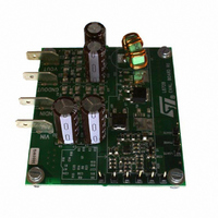
Manufacturer Part Number
STEVAL-ISA037V1
Description
BOARD EVAL BASED ON L6728
Manufacturer
STMicroelectronics
Type
DC/DC Switching Converters, Regulators & Controllersr
Specifications of STEVAL-ISA037V1
Design Resources
STEVAL-ISA037V1 Gerber Files STEVAL-ISA037V1 Schematic STEVAL-ISA037V1 Bill of Material
Main Purpose
DC/DC, Step Down
Outputs And Type
1, Non-Isolated
Voltage - Output
1.25V
Current - Output
20A
Voltage - Input
5 ~ 12V
Regulator Topology
Buck
Frequency - Switching
300kHz
Board Type
Fully Populated
Utilized Ic / Part
L6728
Input Voltage
5 V to 12 V
Output Voltage
1.25 V
Product
Power Management Modules
Silicon Manufacturer
ST Micro
Silicon Core Number
L6728
Kit Application Type
Power Management - Voltage Regulator
Rohs Compliant
Yes
Lead Free Status / RoHS Status
Lead free / RoHS Compliant
Power - Output
-
Lead Free Status / Rohs Status
Lead free / RoHS Compliant
For Use With/related Products
L6728
Other names
497-6418
STEVAL-ISA037V1
STEVAL-ISA037V1


L6728
11
11.1
Application information
Inductor design
The inductance value is defined by a compromise between the dynamic response time, the
efficiency, the cost and the size. The inductor has to be calculated to maintain the ripple
current (ΔI
value can be calculated with the following relationship:
Where F
voltage.
inductor, with V
Increasing the value of the inductance reduces the current ripple but, at the same time,
increases the converter response time to a dynamic load change. The response time is the
time required by the inductor to change its current from initial to final value. Until the inductor
has not finished its charging time, the output current is supplied by the output capacitors.
Minimizing the response time can minimize the output capacitance required. If the
compensation network is well designed, during a load variation the device is able to set a
duty cycle value very different (0 % or 80 %) from steady state one. When this condition is
reached, the response time is limited by the time required to change the inductor current.
Figure 9.
L
=
V
----------------------------- -
F
IN
SW
–
Figure 9
SW
V
⋅
L
ΔI
OUT
) between 20 % and 30 % of the maximum output current (typ). The inductance
is the switching frequency, V
Inductor current ripple vs output voltage
L
⋅
IN
V
--------------
V
shows the ripple current vs. the output voltage for different values of the
OUT
= 5 V and V
IN
IN
= 12 V.
IN
is the input voltage and V
Application information
OUT
is the output
19/31
Related parts for STEVAL-ISA037V1
Image
Part Number
Description
Manufacturer
Datasheet
Request
R

Part Number:
Description:
BOARD RGB CTR ST7,STP08C596MTR
Manufacturer:
STMicroelectronics
Datasheet:

Part Number:
Description:
Power Management IC Development Tools Full Speed USB to RS232 Bridge Demo
Manufacturer:
STMicroelectronics
Datasheet:
Part Number:
Description:
Power Management IC Development Tools 2.5W solar eval BRD USB SPV1040 LD39050
Manufacturer:
STMicroelectronics
Datasheet:

Part Number:
Description:
BOARD EVAL FOR MEMS SENSORS
Manufacturer:
STMicroelectronics
Datasheet:

Part Number:
Description:
KIT DEV STARTER ST10F276Z5
Manufacturer:
STMicroelectronics
Datasheet:

Part Number:
Description:
BOARD EVAL HDMI $ VIDEO SWITCH
Manufacturer:
STMicroelectronics
Datasheet:

Part Number:
Description:
BOARD DEMO ACCELEROMETER DIL24
Manufacturer:
STMicroelectronics
Datasheet:

Part Number:
Description:
BOARD STLM75/STDS75/ST72F651
Manufacturer:
STMicroelectronics
Datasheet:

Part Number:
Description:
EVAL BOARD 3AXIS MEMS ACCELLRMTR
Manufacturer:
STMicroelectronics
Datasheet:

Part Number:
Description:
BOARD EVAL 8BIT MICRO + TDE1708
Manufacturer:
STMicroelectronics
Datasheet:
Part Number:
Description:
STMicroelectronics [RIPPLE-CARRY BINARY COUNTER/DIVIDERS]
Manufacturer:
STMicroelectronics
Datasheet:
Part Number:
Description:
STMicroelectronics [LIQUID-CRYSTAL DISPLAY DRIVERS]
Manufacturer:
STMicroelectronics
Datasheet:
Part Number:
Description:
BOARD EVAL FOR MEMS SENSORS
Manufacturer:
STMicroelectronics
Datasheet: