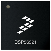
DSP56321VF220 Freescale Semiconductor, DSP56321VF220 Datasheet - Page 41

DSP56321VF220
Manufacturer Part Number
DSP56321VF220
Description
IC DSP 24BIT 220MHZ 196-BGA
Manufacturer
Freescale Semiconductor
Series
DSP563xxr
Type
Fixed Pointr
Datasheet
1.DSP56321VL200R2.pdf
(84 pages)
Specifications of DSP56321VF220
Interface
Host Interface, SSI, SCI
Clock Rate
220MHz
Non-volatile Memory
ROM (576 B)
On-chip Ram
576kB
Voltage - I/o
3.30V
Voltage - Core
1.60V
Operating Temperature
-40°C ~ 100°C
Mounting Type
*
Package / Case
196-MAPBGA
Device Core Size
24b
Format
Fixed Point
Clock Freq (max)
220MHz
Mips
220
Device Input Clock Speed
220MHz
Ram Size
576KB
Operating Supply Voltage (typ)
1.6/3.3V
Operating Supply Voltage (min)
1.5/3/3/3/3/3/3V
Operating Temp Range
-40C to 100C
Operating Temperature Classification
Industrial
Mounting
Surface Mount
Pin Count
196
Package Type
MA-BGA
Package
196MA-BGA
Numeric And Arithmetic Format
Fixed-Point
Maximum Speed
220 MHz
Device Million Instructions Per Second
220 MIPS
Lead Free Status / RoHS Status
Contains lead / RoHS non-compliant
Available stocks
Company
Part Number
Manufacturer
Quantity
Price
Company:
Part Number:
DSP56321VF220
Manufacturer:
XILINX
Quantity:
615
Company:
Part Number:
DSP56321VF220
Manufacturer:
Freescale Semiconductor
Quantity:
10 000
2.4.7
Freescale Semiconductor
Notes:
No.
400 Synchronous clock cycle
401 Clock low period
402 Clock high period
403 Output data setup to
404 Output data hold after
405 Input data setup time
406 Input data not valid
407 Clock falling edge to
408 Output data hold after
409 Input data setup time
410 Input data hold time after
411 Asynchronous clock cycle
412 Clock low period
413 Clock high period
414 Output data setup to
415 Output data hold after
clock falling edge
(internal clock)
clock rising edge (internal
clock)
before clock rising edge
(internal clock)
before clock rising edge
(internal clock)
output data valid (external
clock)
clock rising edge
(external clock)
before clock rising edge
(external clock)
clock rising edge
(external clock)
clock rising edge (internal
clock)
clock rising edge (internal
clock)
Characteristics
1.
2.
3.
4.
SCI Timing
V
t
t
control register and T
In the timing diagrams that follow, the SCLK is drawn using the clock falling edge as a the first reference. Clock polarity is
programmable in the SCI Control Register (SCR). Refer to the DSP56321 Reference Manual for details.
SCC
ACC
CCQH
= synchronous clock cycle time (for internal clock, t
= asynchronous clock cycle time; value given for 1X Clock mode (for internal clock, t
= 3.3 V ± 0.3 V, V
1
Symbol
t
t
C
SCC
ACC
).
CCQL
2
3
t
= 1.6 V ± 0.1 V; T
t
SCC
t
SCC
SCC
t
SCC
/4 + 0.5 × T
DSP56321 Technical Data, Rev. 11
/4 + 0.5 × T
Expression
/4 + 0.5 × T
t
t
t
t
t
t
SCC
SCC
ACC
ACC
ACC
ACC
T
16 × T
/4 − 1.5 × T
64 × T
Table 2-11.
C
/2 − 10.0
/2 − 10.0
/2 − 10.0
/2 − 10.0
/2 − 30.0
/2 − 30.0
+ 8.0
C
C
C
C
C
+ 25.0
J
− 17.0
− 5.5
C
= –40°C to +100 °C, C
SCC
320.0
150.0
150.0
130.0
130.0
SCI Timings
Min
80.0
30.0
30.0
47.5
13.0
5.5
0.0
9.0
13
200 MHz
—
—
is determined by the SCI clock control register and T
Max
17.0
32.0
—
—
—
—
—
—
—
—
—
—
—
—
—
—
L
291.2
135.6
135.6
115.6
115.6
Min
72.8
26.4
26.4
11.5
45.5
12.6
= 50 pF.
3.5
0.0
9.0
220 MHz
—
—
Max
15.0
32.0
—
—
—
—
—
—
—
—
—
—
—
—
—
—
266.9
123.5
123.5
103.5
103.5
ACC
Min
66.7
23.4
23.4
1.76
43.8
12.2
0.0
9.0
10
—
—
240 MHz
AC Electrical Characteristics
is determined by the SCI clock
Max
13.8
32.0
—
—
—
—
—
—
—
—
—
—
—
—
—
—
–0.68
41.32
11.64
232.0
106.0
106.0
Min
58.0
19.0
19.0
9.04
86.0
86.0
0.0
9.0
—
—
275 MHz
C
10.81
Max
32.0
).
—
—
—
—
—
—
—
—
—
—
—
—
—
—
Uni
2-21
ns
ns
ns
ns
ns
ns
ns
ns
ns
ns
ns
ns
ns
ns
ns
ns
t


