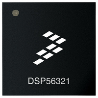
DSP56321VF220 Freescale Semiconductor, DSP56321VF220 Datasheet - Page 47

DSP56321VF220
Manufacturer Part Number
DSP56321VF220
Description
IC DSP 24BIT 220MHZ 196-BGA
Manufacturer
Freescale Semiconductor
Series
DSP563xxr
Type
Fixed Pointr
Datasheet
1.DSP56321VL200R2.pdf
(84 pages)
Specifications of DSP56321VF220
Interface
Host Interface, SSI, SCI
Clock Rate
220MHz
Non-volatile Memory
ROM (576 B)
On-chip Ram
576kB
Voltage - I/o
3.30V
Voltage - Core
1.60V
Operating Temperature
-40°C ~ 100°C
Mounting Type
*
Package / Case
196-MAPBGA
Device Core Size
24b
Format
Fixed Point
Clock Freq (max)
220MHz
Mips
220
Device Input Clock Speed
220MHz
Ram Size
576KB
Operating Supply Voltage (typ)
1.6/3.3V
Operating Supply Voltage (min)
1.5/3/3/3/3/3/3V
Operating Temp Range
-40C to 100C
Operating Temperature Classification
Industrial
Mounting
Surface Mount
Pin Count
196
Package Type
MA-BGA
Package
196MA-BGA
Numeric And Arithmetic Format
Fixed-Point
Maximum Speed
220 MHz
Device Million Instructions Per Second
220 MIPS
Lead Free Status / RoHS Status
Contains lead / RoHS non-compliant
Available stocks
Company
Part Number
Manufacturer
Quantity
Price
Company:
Part Number:
DSP56321VF220
Manufacturer:
XILINX
Quantity:
615
Company:
Part Number:
DSP56321VF220
Manufacturer:
Freescale Semiconductor
Quantity:
10 000
2.4.10 Considerations For GPIO Use
The following considerations can be helpful when GPIO is used.
2.4.10.1 GPIO as Output
2.4.10.2 GPIO as Input
GPIO inputs are not synchronized with the core clock. When only one GPIO bit is polled, this lack of
synchronization presents no problem, since the read value can be either the previous value or the new value of the
corresponding GPIO pin. However, there is the risk of reading an intermediate state if:
Therefore, when GPIO bits are read, the recommended practice is to poll continuously until two consecutive read
operations have identical results.
Freescale Semiconductor
•
•
•
•
The time from fetch of the instruction that changes the GPIO pin to the actual change is seven core clock
cycles, if the instruction is a on
delays.
The maximum rise or fall time of a GPIO pin is 13 ns (TTL levels, assuming that the maximum of 50 pF
load limit is met).
Two or more GPIO bits are treated as a coupled group (for example, four possible status states encoded in
two bits).
The read operation occurs during a simultaneous change of GPIO pins (for example, the change of 00 to 11
may happen through an intermediate state of 01 or 10).
TIO
TIO (Input)
Address
Figure 2-26.
Figure 2-27.
e
-cycle instruction and there are no pipeline stalls or any other pipeline
480
DSP56321 Technical Data, Rev. 11
TIO Timer Event Input Restrictions
Timer Interrupt Generation
481
First Interrupt Instruction Execution
486
AC Electrical Characteristics
2-27


