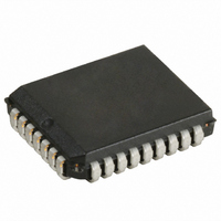
CY7C4261-10JC Cypress Semiconductor Corp, CY7C4261-10JC Datasheet - Page 4

CY7C4261-10JC
Manufacturer Part Number
CY7C4261-10JC
Description
IC DEEP SYNC FIFO 16KX9 32-PLCC
Manufacturer
Cypress Semiconductor Corp
Series
CY7Cr
Datasheet
1.CY7C4261-10JC.pdf
(18 pages)
Specifications of CY7C4261-10JC
Function
Synchronous
Memory Size
144K (16K x 9)
Data Rate
100MHz
Access Time
8ns
Voltage - Supply
3.3V
Operating Temperature
-40°C ~ 85°C
Mounting Type
Surface Mount
Package / Case
32-PLCC
Lead Free Status / RoHS Status
Contains lead / RoHS non-compliant
Other names
428-1232
Document #: 38-06015 Rev. *B
Table 1. Writing the Offset Registers
Table 2. Status Flags
Width-Expansion Configuration
Word width may be increased simply by connecting the corre-
sponding input controls signals of multiple devices. A
composite flag should be created for each of the end-point
status flags (EF and FF). The partial status flags (PAE and PAF)
can be detected from any one device. Figure 2 demonstrates
a 18-bit word width by using two CY7C4261/71s. Any word
width can be attained by adding additional CY7C4261/71s.
When the CY7C4261/71 is in a Width-Expansion Configu-
ration, the Read Enable (REN2) control input can be grounded
(see Figure 2). In this configuration, the Write Enable 2/Load
(WEN2/LD) pin is set to LOW at Reset so that the pin operates
as a control to load and read the programmable flag offsets.
Note:
0
1 to n
(n+1) to (16384
(16384
16384
1.
2.
3.
LD
0
0
1
1
The same selection sequence applies to reading from the registers. REN1 and REN2 are enabled and a read is performed on the LOW-to-HIGH transition of RCLK.
n = Empty Offset (n = 7 default value).
m = Full Offset (m = 7 default value).
[2]
WEN
m)
0
1
0
1
[3]
to 16383
CY7C4261
WCLK
(m+1))
[1]
Number of Words in FIFO
No Operation
Write Into FIFO
No Operation
Empty Offset (LSB)
Empty Offset (MSB)
Full Offset (LSB)
Full Offset (MSB)
Selection
0
1 to n
(n+1) to (32768
(32768
32768
[2]
m)
[3]
to 32767
CY7C4271
(m+1))
The number formed by the empty offset least significant bit
register and empty offset most significant bit register is
referred to as n and determines the operation of PAE. PAF is
synchronized to the LOW-to-HIGH transition of RCLK by one
flip-flop and is LOW when the FIFO contains n or fewer unread
words. PAE is set HIGH by the LOW-to-HIGH transition of
RCLK when the FIFO contains (n+1) or greater unread words.
The number formed by the full offset least significant bit
register and full offset most significant bit register is referred to
as m and determines the operation of PAF. PAE is synchronized
to the LOW-to-HIGH transition of WCLK by one flip-flop and is
set LOW when the number of unread words in the FIFO is
greater than or equal to CY7C4261 (16K-m) and CY7C4271
(32K-m). PAF is set HIGH by the LOW-to-HIGH transition of
WCLK when the number of available memory locations is
greater than m.
Flag Operation
The CY7C4261/71 devices provide four flag pins to indicate
the condition of the FIFO contents. Empty, Full, PAE, and PAF
are synchronous.
Full Flag
The Full Flag (FF) will go LOW when the device is full. Write
operations are inhibited whenever FF is LOW regardless of the
state of WEN1 and WEN2/LD. FF is synchronized to WCLK, i.e.,
it is exclusively updated by each rising edge of WCLK.
Empty Flag
The Empty Flag (EF) will go LOW when the device is empty.
Read operations are inhibited whenever EF is LOW,
regardless of the state of REN1 and REN2. EF is synchronized
to RCLK, i.e., it is exclusively updated by each rising edge of
RCLK.
FF
H
H
H
H
L
PAF
H
H
H
L
L
CY7C4261
CY7C4271
PAE
H
H
H
L
L
Page 4 of 18
EF
H
H
H
H
L


