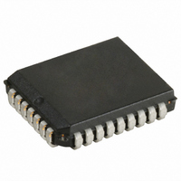
CY7C4261-10JC Cypress Semiconductor Corp, CY7C4261-10JC Datasheet - Page 9

CY7C4261-10JC
Manufacturer Part Number
CY7C4261-10JC
Description
IC DEEP SYNC FIFO 16KX9 32-PLCC
Manufacturer
Cypress Semiconductor Corp
Series
CY7Cr
Datasheet
1.CY7C4261-10JC.pdf
(18 pages)
Specifications of CY7C4261-10JC
Function
Synchronous
Memory Size
144K (16K x 9)
Data Rate
100MHz
Access Time
8ns
Voltage - Supply
3.3V
Operating Temperature
-40°C ~ 85°C
Mounting Type
Surface Mount
Package / Case
32-PLCC
Lead Free Status / RoHS Status
Contains lead / RoHS non-compliant
Other names
428-1232
Document #: 38-06015 Rev. *B
WEN2/LD
Switching Waveforms
Notes:
16. The clocks (RCLK, WCLK) can be free-running during reset.
17. After reset, the outputs will be LOW if OE = 0 and three-state if OE=1.
18. Holding WEN2/LD HIGH during reset will make the pin act as a second enable pin. Holding WEN2/LD LOW during reset will make the pin act as a load enable for the
19. When t
20. The first word is available the cycle after EF goes HIGH, always.
Reset Timing
First Data Word Latency after Reset with Read and Write
(if applicable)
programmable flag offset registers.
The Latency Timing applies only at the Empty Boundary (EF = LOW).
Q
EF,PAE
FF,PAF
Q
D
WEN2
REN1,
WEN1
WEN1
0 -
WCLK
REN1,
REN2
RCLK
0
0
REN2
RS
–D
–Q
OE
[18]
EF
Q
SKEW1
8
8
8
> minimum specification, t
[16]
t
ENS
t
DS
D
0
(FIRST VALID WRITE)
(continued)
FRL
(maximum) = t
t
SKEW1
t
t
t
RSF
RSF
RSF
t
RS
t
OLZ
t
FRL
CLK
t
t
t
RSS
RSS
RSS
+ t
[19]
SKEW2
. When t
t
D
REF
1
SKEW2
t
OE
< minimum specification, t
t
D
A
t
t
t
[20]
RSR
RSR
RSR
2
FRL
(maximum) = either 2*t
D
0
t
A
D
3
CLK
+ t
OE=0
O
SKEW1
CY7C4261
CY7C4271
E
=1
[17]
or t
Page 9 of 18
D
CLK
1
D
4
+ t
SKEW1
.


