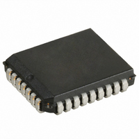
CY7C4261-10JC Cypress Semiconductor Corp, CY7C4261-10JC Datasheet - Page 6

CY7C4261-10JC
Manufacturer Part Number
CY7C4261-10JC
Description
IC DEEP SYNC FIFO 16KX9 32-PLCC
Manufacturer
Cypress Semiconductor Corp
Series
CY7Cr
Datasheet
1.CY7C4261-10JC.pdf
(18 pages)
Specifications of CY7C4261-10JC
Function
Synchronous
Memory Size
144K (16K x 9)
Data Rate
100MHz
Access Time
8ns
Voltage - Supply
3.3V
Operating Temperature
-40°C ~ 85°C
Mounting Type
Surface Mount
Package / Case
32-PLCC
Lead Free Status / RoHS Status
Contains lead / RoHS non-compliant
Other names
428-1232
Document #: 38-06015 Rev. *B
Maximum Ratings
(Above which the useful life may be impaired. For user guide-
lines, not tested.)
Storage Temperature
Ambient Temperature with
Power Applied
Supply Voltage to Ground Potential
DC Voltage Applied to Outputs
in High-Z State
Electrical Characteristics
Capacitance
AC Test Loads and Waveforms
Notes:
10. CL = 30 pF for all AC parameters except for t
11. CL = 5 pF for t
V
V
V
V
V
I
I
I
I
I
C
C
4.
5.
6.
7.
8.
9.
Parameter
IX
OZL
OZH
CC1
SB
Equivalent to:
OH
OL
IH
IH
IL
IN
OUT
[8]
The voltage on any input or I/O pin cannot exceed the power pin during power-up.
TA is the “instant on” case temperature.
See the last page of this specification for Group A subgroup testing information.
Input signals switch from 0V to 3V with a rise/fall time of less than 3 ns, clocks and clock enables switch at maximum frequency 20 Mhz, while data inputs switch
at 10 MHz. Outputs are unloaded. I
All inputs = V
Tested initially and after any design or process changes that may affect these parameters.
[7]
Parameter
Output HIGH Voltage V
Output LOW Voltage
Input HIGH Voltage
(comm./ind.)
Input HIGH Voltage
(military)
Input LOW Voltage
Input Leakage Current V
Output OFF,
High Z Current
Active Power Supply
Current
Average Standby
Current
OUTPUT
CC
OUTPUT
OHZ
[9]
INCLUDING
– 0.2V, except WCLK and RCLK (which are switching at frequency = 20 MHz). All outputs are unloaded.
Description
.
JIG AND
THÉVENIN EQUIVALENT
SCOPE
5V
[4]
Input Capacitance
Output Capacitance
C
L
CC1
420
Over the Operating Range
R11.1KW
(typical) = (20 mA + (freq – 20 MHz) * (0.7 mA/MHz)).
Description
I
V
I
OE
V
Test Conditions
OH
OL
CC
CC
CC
SS
OHZ
= 8.0 mA
= 2.0 mA
[10, 11]
= Max.
0.5V to V
= Min.,
= Min.,
< V
R2
680
.
V
IH
1.91V
O
65 C to +150 C
55 C to +125 C
Com’l
Ind/Mil
Com’l
Ind/Mil
,
< V
0.5V to +7.0V
CC
CC
+ 0.5V
7C4261/71 10 7C4261/71 15 7C4261/71 25 7C4261/71 35
Min.
2.4
2.0
2.2
T
V
0.5
10
10
A
CC
[6]
= 25 C, f = 1 MHz,
= 5.0V
Max.
V
V
Test Conditions
DC Input Voltage.......................................... 0.5V to V
Output Current into Outputs (LOW)............................. 20 mA
Static Discharge Voltage............................................ >2001V
(per MIL-STD-883, Method 3015)
Latch-up Current...................................................... >200 mA
Operating Range
+10
+10
0.4
0.8
Commercial
Industrial
Military
35
40
10
15
CC
CC
GND
3.0V
Range
Min.
2.4
2.0
2.2
0.5
10
10
[5]
3 ns
Max.
V
V
+10
+10
0.4
0.8
35
40
10
15
CC
CC
Ambient Temperature
ALL INPUT PULSES
10%
90%
Min.
55 C to +125 C
2.4
2.0
2.2
0 C to +70 C
40 C to +85 C
0.5
10
10
Max.
Max.
V
V
+10
+10
0.4
0.8
35
40
10
15
5
7
CC
CC
90%
Min.
2.4
2.0
2.2
0.5
10%
10
10
CY7C4261
CY7C4271
3 ns
Page 6 of 18
Max.
5V 10%
5V 10%
5V 10%
V
V
+10
+10
0.4
0.8
35
40
10
15
CC
CC
Unit
V
pF
pF
CC
cc
+0.5V
Unit
mA
mA
mA
mA
V
V
V
V
V
A
A


