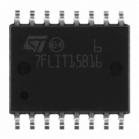
ST7FLIT15BY1M6 STMicroelectronics, ST7FLIT15BY1M6 Datasheet - Page 140

ST7FLIT15BY1M6
Manufacturer Part Number
ST7FLIT15BY1M6
Description
IC MCU 8BIT 4K FLASH 16-SOIC
Manufacturer
STMicroelectronics
Series
ST7r
Datasheet
1.ST7FLIT15BY1M6.pdf
(159 pages)
Specifications of ST7FLIT15BY1M6
Core Processor
ST7
Core Size
8-Bit
Speed
8MHz
Connectivity
SPI
Peripherals
LVD, POR, PWM, WDT
Number Of I /o
11
Program Memory Size
4KB (4K x 8)
Program Memory Type
FLASH
Ram Size
256 x 8
Voltage - Supply (vcc/vdd)
2.7 V ~ 5.5 V
Data Converters
A/D 7x10b
Oscillator Type
Internal
Operating Temperature
-40°C ~ 85°C
Package / Case
16-SOIC (0.300", 7.5mm Width)
Controller Family/series
ST7
No. Of I/o's
13
Ram Memory Size
256Byte
Cpu Speed
8MHz
No. Of Timers
5
Rohs Compliant
Yes
Processor Series
ST7FLIT1x
Core
ST7
Data Bus Width
8 bit
Data Ram Size
256 B
Interface Type
SPI
Maximum Clock Frequency
8 MHz
Number Of Programmable I/os
17
Number Of Timers
4
Maximum Operating Temperature
+ 85 C
Mounting Style
SMD/SMT
Development Tools By Supplier
ST7FLITE-SK/RAIS, ST7MDT10-DVP3, ST7MDT10-EMU3, STX-RLINK
Minimum Operating Temperature
- 40 C
On-chip Adc
10 bit, 7 Channel
For Use With
497-5049 - KIT STARTER RAISONANCE ST7FLITE497-5046 - KIT TOOL FOR ST7/UPSD/STR7 MCU
Lead Free Status / RoHS Status
Lead free / RoHS Compliant
Eeprom Size
-
Lead Free Status / Rohs Status
Details
Other names
497-8245-5
ST7FLIT15BY1M6
ST7FLIT15BY1M6
Available stocks
Company
Part Number
Manufacturer
Quantity
Price
ST7LITE1xB
ADC CHARACTERISTICS (Cont’d)
ADC Accuracy with V
Notes:
1. Data based on characterization results. Not tested in production.
2. Injecting negative current on any of the analog input pins significantly reduces the accuracy of any conversion being
performed on any analog input.
Analog pins can be protected against negative injection by adding a Schottky diode (pin to ground). Injecting negative
current on digital input pins degrades ADC accuracy especially if performed on a pin close to the analog input pins.
Any positive injection current within the limits specified for I
ADC accuracy.
3. Data based on characterization results over the whole temperature range, monitored in production.
Figure 111. ADC Accuracy Characteristics with amplifier disabled
140/159
Symbol
1023
1022
1021
E
E
E
E
E
7
6
5
4
3
2
1
O
G
0
D
T
L
V
SS
Digital Result ADCDR
1LSB
1
Total unadjusted error
Offset error
Gain Error
Differential linearity error
Integral linearity error
E
O
2
IDEAL
3
=
V
------------------------------- -
4
DD
Parameter
DD
1024
=5.0V
–
5
1 LSB
V
SS
3)
E
6
T
IDEAL
3)
E
7
L
(2)
E
D
1021 1022 1023 1024
(3)
f
CPU
(1)
=8MHz, f
INJ
E
Conditions
(PIN) and ΣI
G
V
DD
ADC
(1) Example of an actual transfer curve
(2) The ideal transfer curve
(3) End point correlation line
E
between the actual and the ideal transfer curves.
E
transition and the first ideal one.
E
transition and the last actual one.
E
between actual steps and the ideal one.
E
between any actual transition and the end point
correlation line.
=4MHz
T
O
G
D
L
=Total Unadjusted Error: maximum deviation
=Integral Linearity Error: maximum deviation
=Differential Linearity Error: maximum deviation
=Offset Error: deviation between the first actual
=Gain Error: deviation between the last ideal
INJ
V
in
(PIN) in
(LSB
IDEAL
Section 13.8
Typ
)
0.5
1.5
1.5
4
3
does not affect the
Max
6
5
4
3
3
1)
1)
1)
2)
2)
Unit
LSB


