ST7FLIT15BY1M6 STMicroelectronics, ST7FLIT15BY1M6 Datasheet - Page 98
ST7FLIT15BY1M6
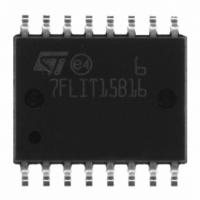
Manufacturer Part Number
ST7FLIT15BY1M6
Description
IC MCU 8BIT 4K FLASH 16-SOIC
Manufacturer
STMicroelectronics
Series
ST7r
Datasheet
1.ST7FLIT15BY1M6.pdf
(159 pages)
Specifications of ST7FLIT15BY1M6
Core Processor
ST7
Core Size
8-Bit
Speed
8MHz
Connectivity
SPI
Peripherals
LVD, POR, PWM, WDT
Number Of I /o
11
Program Memory Size
4KB (4K x 8)
Program Memory Type
FLASH
Ram Size
256 x 8
Voltage - Supply (vcc/vdd)
2.7 V ~ 5.5 V
Data Converters
A/D 7x10b
Oscillator Type
Internal
Operating Temperature
-40°C ~ 85°C
Package / Case
16-SOIC (0.300", 7.5mm Width)
Controller Family/series
ST7
No. Of I/o's
13
Ram Memory Size
256Byte
Cpu Speed
8MHz
No. Of Timers
5
Rohs Compliant
Yes
Processor Series
ST7FLIT1x
Core
ST7
Data Bus Width
8 bit
Data Ram Size
256 B
Interface Type
SPI
Maximum Clock Frequency
8 MHz
Number Of Programmable I/os
17
Number Of Timers
4
Maximum Operating Temperature
+ 85 C
Mounting Style
SMD/SMT
Development Tools By Supplier
ST7FLITE-SK/RAIS, ST7MDT10-DVP3, ST7MDT10-EMU3, STX-RLINK
Minimum Operating Temperature
- 40 C
On-chip Adc
10 bit, 7 Channel
For Use With
497-5049 - KIT STARTER RAISONANCE ST7FLITE497-5046 - KIT TOOL FOR ST7/UPSD/STR7 MCU
Lead Free Status / RoHS Status
Lead free / RoHS Compliant
Eeprom Size
-
Lead Free Status / Rohs Status
Details
Other names
497-8245-5
ST7FLIT15BY1M6
ST7FLIT15BY1M6
Available stocks
Company
Part Number
Manufacturer
Quantity
Price


ST7LITE1xB
10-BIT A/D CONVERTER (ADC) (Cont’d)
11.5.6 Register Description
CONTROL/STATUS REGISTER (ADCCSR)
Read/Write (Except bit 7 read only)
Reset Value: 0000 0000 (00h)
Bit 7 = EOC End of Conversion
This bit is set by hardware. It is cleared by hard-
ware when software reads the ADCDRH register
or writes to any bit of the ADCCSR register.
0: Conversion is not complete
1: Conversion complete
Bit 6 = SPEED ADC clock selection
This bit is set and cleared by software. It is used
together with the SLOW bit to configure the ADC
clock speed. Refer to the table in the SLOW bit de-
scription (ADCDRL register).
Bit 5 = ADON A/D Converter on
This bit is set and cleared by software.
0: A/D converter and amplifier are switched off
1: A/D converter and amplifier are switched on
Bits 4:3 = Reserved. Must be kept cleared.
Bits 2:0 = CH[2:0] Channel Selection
These bits are set and cleared by software. They
select the analog input to convert.
*The number of channels is device dependent. Refer to
the device pinout description.
98/159
1
EOC SPEED ADON
7
Channel Pin*
AIN0
AIN1
AIN2
AIN3
AIN4
AIN5
AIN6
0
0
CH2
0
0
0
0
1
1
1
CH2
CH1
CH1
0
0
1
1
0
0
1
CH0
CH0
0
1
0
1
0
1
0
0
DATA REGISTER HIGH (ADCDRH)
Read Only
Reset Value: xxxx xxxx (xxh)
Bits 7:0 = D[9:2] MSB of Analog Converted Value
AMP CONTROL/DATA REGISTER LOW (AD-
CDRL)
Read/Write
Reset Value: 0000 00xx (0xh)
Bits 7:5 = Reserved. Forced by hardware to 0.
Bit 4 = AMPCAL Amplifier Calibration Bit
This bit is set and cleared by software. It is advised
to use this bit to calibrate the ADC when amplifier
is ON. Setting this bit internally connects amplifier
input to 0V. Hence, corresponding ADC output can
be used in software to eliminate amplifier-offset er-
ror.
0: Calibration off
1: Calibration on. (The input voltage of the amplifi-
er is set to 0V)
Bit 3 = SLOW Slow mode
This bit is set and cleared by software. It is used
together with the SPEED bit in the ADCCSR regis-
ter to configure the ADC clock speed as shown on
the table below.
Note: max f
13.11 on page
D9
7
7
0
D8
0
ADC
D7
f
f
139)
0
f
CPU
CPU
f
ADC
CPU
allowed = 4MHz (see
/2
/4
AMP
CAL
D6
SLOW
D5
AMP-
SEL
D4
SLOW SPEED
0
0
1
D3
D1
section
D2
D0
0
1
x
0
0
Related parts for ST7FLIT15BY1M6
Image
Part Number
Description
Manufacturer
Datasheet
Request
R

Part Number:
Description:
STMicroelectronics [RIPPLE-CARRY BINARY COUNTER/DIVIDERS]
Manufacturer:
STMicroelectronics
Datasheet:
Part Number:
Description:
STMicroelectronics [LIQUID-CRYSTAL DISPLAY DRIVERS]
Manufacturer:
STMicroelectronics
Datasheet:

Part Number:
Description:
BOARD EVAL FOR MEMS SENSORS
Manufacturer:
STMicroelectronics
Datasheet:
Part Number:
Description:
NPN TRANSISTOR POWER MODULE
Manufacturer:
STMicroelectronics
Datasheet:
Part Number:
Description:
TURBOSWITCH ULTRA-FAST HIGH VOLTAGE DIODE
Manufacturer:
STMicroelectronics
Datasheet:
Part Number:
Description:
Manufacturer:
STMicroelectronics
Datasheet:
Part Number:
Description:
DIODE / SCR MODULE
Manufacturer:
STMicroelectronics
Datasheet:
Part Number:
Description:
DIODE / SCR MODULE
Manufacturer:
STMicroelectronics
Datasheet:
Part Number:
Description:
Search -----> STE16N100
Manufacturer:
STMicroelectronics
Datasheet:
Part Number:
Description:
Search ---> STE53NA50
Manufacturer:
STMicroelectronics
Datasheet:
Part Number:
Description:
NPN Transistor Power Module
Manufacturer:
STMicroelectronics
Datasheet:
Part Number:
Description:
DIODE / SCR MODULE
Manufacturer:
STMicroelectronics
Datasheet: