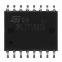
ST7FLIT15BY1M6 STMicroelectronics, ST7FLIT15BY1M6 Datasheet - Page 76

ST7FLIT15BY1M6
Manufacturer Part Number
ST7FLIT15BY1M6
Description
IC MCU 8BIT 4K FLASH 16-SOIC
Manufacturer
STMicroelectronics
Series
ST7r
Datasheet
1.ST7FLIT15BY1M6.pdf
(159 pages)
Specifications of ST7FLIT15BY1M6
Core Processor
ST7
Core Size
8-Bit
Speed
8MHz
Connectivity
SPI
Peripherals
LVD, POR, PWM, WDT
Number Of I /o
11
Program Memory Size
4KB (4K x 8)
Program Memory Type
FLASH
Ram Size
256 x 8
Voltage - Supply (vcc/vdd)
2.7 V ~ 5.5 V
Data Converters
A/D 7x10b
Oscillator Type
Internal
Operating Temperature
-40°C ~ 85°C
Package / Case
16-SOIC (0.300", 7.5mm Width)
Controller Family/series
ST7
No. Of I/o's
13
Ram Memory Size
256Byte
Cpu Speed
8MHz
No. Of Timers
5
Rohs Compliant
Yes
Processor Series
ST7FLIT1x
Core
ST7
Data Bus Width
8 bit
Data Ram Size
256 B
Interface Type
SPI
Maximum Clock Frequency
8 MHz
Number Of Programmable I/os
17
Number Of Timers
4
Maximum Operating Temperature
+ 85 C
Mounting Style
SMD/SMT
Development Tools By Supplier
ST7FLITE-SK/RAIS, ST7MDT10-DVP3, ST7MDT10-EMU3, STX-RLINK
Minimum Operating Temperature
- 40 C
On-chip Adc
10 bit, 7 Channel
For Use With
497-5049 - KIT STARTER RAISONANCE ST7FLITE497-5046 - KIT TOOL FOR ST7/UPSD/STR7 MCU
Lead Free Status / RoHS Status
Lead free / RoHS Compliant
Eeprom Size
-
Lead Free Status / Rohs Status
Details
Other names
497-8245-5
ST7FLIT15BY1M6
ST7FLIT15BY1M6
Available stocks
Company
Part Number
Manufacturer
Quantity
Price
ST7LITE1xB
DUAL 12-BIT AUTORELOAD TIMER 4 (Cont’d)
Bit 1= TRAN2 Transfer enable2
This bit is read/write by software, cleared by hard-
ware after each completed transfer and set by
hardware after reset. It controls the transfers on
CNTR2.
It allows the value of the Preload DCRx registers
to be transferred to the Active DCRx registers after
the next overflow event.
The OPx bits are transferred to the shadow OPx
bits in the same way.
Notes:
1. DCR2/3 transfer will be controlled using this bit
if ENCNTR2 bit is set.
2. This bit must not be reset by software
Bit 0 = TRAN1 Transfer enable 1
This bit is read/write by software, cleared by hard-
ware after each completed transfer and set by
hardware after reset. It controls the transfers on
CNTR1. It allows the value of the Preload DCRx
registers to be transferred to the Active DCRx reg-
isters after the next overflow event.
The OPx bits are transferred to the shadow OPx
bits in the same way.
Notes:
1. DCR0,1 transfers are always controlled using
this bit.
2. DCR2/3 transfer will be controlled using this bit
if ENCNTR2 is reset.
3.This bit must not be reset by software
AUTORELOAD REGISTER2 (ATR2H)
Read / Write
Reset Value: 0000 0000 (00h)
76/159
1
15
0
0
0
0
ATR11 ATR10 ATR9
ATR8
8
AUTORELOAD REGISTER (ATR2L)
Read / Write
Reset Value: 0000 0000 (00h)
Bits 11:0 = ATR2[11:0] Autoreload Register 2.
This is a 12-bit register which is written by soft-
ware. The ATR2 register value is automatically
loaded into the upcounter CNTR2 when an over-
flow of CNTR2 occurs. The register value is used
to
ENCNTR2 is set.
DEAD TIME GENERATOR REGISTER (DTGR)
Read/Write
Reset Value: 0000 0000 (00h)
Bit 7 = DTE Dead Time Enable
This bit is read/write by software. It enables a dead
time generation on PWM0/PWM1.
0: No Dead time insertion.
1: Dead time insertion enabled.
Bits 6:0 = DT[6:0] Dead Time Value
These bits are read/write by software. They define
the dead time inserted between PWM0/PWM1.
Dead time is calculated as follows:
Dead Time = DT[6:0] x Tcounter1
Note:
1. If DTE is set and DT[6:0]=0, PWM output sig-
nals will be at their reset state.
ATR7
DTE
7
7
set
ATR6
DT6
the
ATR5
DT5
PWM2/PWM3
ATR4
DT4
ATR3
DT3
frequency
ATR2
DT2
ATR1
DT1
when
ATR0
DT0
0
0


