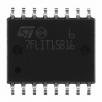
ST7FLIT15BY1M6 STMicroelectronics, ST7FLIT15BY1M6 Datasheet - Page 89

ST7FLIT15BY1M6
Manufacturer Part Number
ST7FLIT15BY1M6
Description
IC MCU 8BIT 4K FLASH 16-SOIC
Manufacturer
STMicroelectronics
Series
ST7r
Datasheet
1.ST7FLIT15BY1M6.pdf
(159 pages)
Specifications of ST7FLIT15BY1M6
Core Processor
ST7
Core Size
8-Bit
Speed
8MHz
Connectivity
SPI
Peripherals
LVD, POR, PWM, WDT
Number Of I /o
11
Program Memory Size
4KB (4K x 8)
Program Memory Type
FLASH
Ram Size
256 x 8
Voltage - Supply (vcc/vdd)
2.7 V ~ 5.5 V
Data Converters
A/D 7x10b
Oscillator Type
Internal
Operating Temperature
-40°C ~ 85°C
Package / Case
16-SOIC (0.300", 7.5mm Width)
Controller Family/series
ST7
No. Of I/o's
13
Ram Memory Size
256Byte
Cpu Speed
8MHz
No. Of Timers
5
Rohs Compliant
Yes
Processor Series
ST7FLIT1x
Core
ST7
Data Bus Width
8 bit
Data Ram Size
256 B
Interface Type
SPI
Maximum Clock Frequency
8 MHz
Number Of Programmable I/os
17
Number Of Timers
4
Maximum Operating Temperature
+ 85 C
Mounting Style
SMD/SMT
Development Tools By Supplier
ST7FLITE-SK/RAIS, ST7MDT10-DVP3, ST7MDT10-EMU3, STX-RLINK
Minimum Operating Temperature
- 40 C
On-chip Adc
10 bit, 7 Channel
For Use With
497-5049 - KIT STARTER RAISONANCE ST7FLITE497-5046 - KIT TOOL FOR ST7/UPSD/STR7 MCU
Lead Free Status / RoHS Status
Lead free / RoHS Compliant
Eeprom Size
-
Lead Free Status / Rohs Status
Details
Other names
497-8245-5
ST7FLIT15BY1M6
ST7FLIT15BY1M6
Available stocks
Company
Part Number
Manufacturer
Quantity
Price
SERIAL PERIPHERAL INTERFACE (cont’d)
11.4.4 Clock Phase and Clock Polarity
Four possible timing relationships may be chosen
by software, using the CPOL and CPHA bits (See
Figure
Note: The idle state of SCK must correspond to
the polarity selected in the SPICSR register (by
pulling up SCK if CPOL = 1 or pulling down SCK if
CPOL = 0).
The combination of the CPOL clock polarity and
CPHA (clock phase) bits selects the data capture
clock edge.
Figure 57. Data Clock Timing Diagram
5).
(from slave)
(from slave)
(to slave)
(to slave)
(from master)
(from master)
MISO
MOSI
CAPTURE STROBE
SCK
(CPOL = 1)
SCK
(CPOL = 0)
MISO
MOSI
CAPTURE STROBE
SCK
(CPOL = 1)
SCK
(CPOL = 0)
SS
SS
Note: This figure should not be used as a replacement for parametric information.
Refer to the Electrical Characteristics chapter.
MSBit
MSBit
MSBit
MSBit
Bit 6
Bit 6
Bit 6
Bit 6
Bit 5
Bit 5
Bit 5
Bit 5
CPHA = 0
CPHA = 1
Bit 4
Bit 4
Bit 4
Bit 4
Figure 5
binations of the CPHA and CPOL bits. The dia-
gram may be interpreted as a master or slave tim-
ing diagram where the SCK pin, the MISO pin and
the MOSI pin are directly connected between the
master and the slave device.
Note: If CPOL is changed at the communication
byte boundaries, the SPI must be disabled by re-
setting the SPE bit.
Bit3
Bit3
Bit3
Bit3
shows an SPI transfer with the four com-
Bit 2
Bit 2
Bit 2
Bit 2
Bit 1
Bit 1
Bit 1
Bit 1
LSBit
LSBit
LSBit
LSBit
ST7LITE1xB
89/159
1


