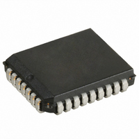
CY7C4261V-15JXC Cypress Semiconductor Corp, CY7C4261V-15JXC Datasheet - Page 8

CY7C4261V-15JXC
Manufacturer Part Number
CY7C4261V-15JXC
Description
IC SYNC FIFO MEM 16KX9 32-PLCC
Manufacturer
Cypress Semiconductor Corp
Series
CY7Cr
Datasheet
1.CY7C4281V-10JXC.pdf
(22 pages)
Specifications of CY7C4261V-15JXC
Access Time
10ns
Memory Size
144K (16K x 9)
Package / Case
32-PLCC
Function
Synchronous
Data Rate
100MHz
Voltage - Supply
3.3V
Operating Temperature
-40°C ~ 85°C
Mounting Type
Surface Mount
Number Of Circuits
2
Data Bus Width
9 bit
Bus Direction
Unidirectional
Timing Type
Synchronous
Organization
16 K x 9
Maximum Clock Frequency
66.7 MHz
Supply Voltage (max)
3.6 V
Supply Voltage (min)
3 V
Maximum Operating Current
25 mA
Maximum Operating Temperature
+ 70 C
Minimum Operating Temperature
0 C
Mounting Style
SMD/SMT
Lead Free Status / RoHS Status
Lead free / RoHS Compliant
Lead Free Status / RoHS Status
Lead free / RoHS Compliant, Lead free / RoHS Compliant
Available stocks
Company
Part Number
Manufacturer
Quantity
Price
Company:
Part Number:
CY7C4261V-15JXC
Manufacturer:
Cypress Semiconductor Corp
Quantity:
10 000
Maximum Ratings
(Exceeding maximum ratings may shorten the useful life of the
device. User guidelines are not tested.)
Storage temperature .................................. –65 °C to +150 °C
Ambient temperature with power applied ... –55 °C to +125 °C
Supply voltage to ground potential ...............–0.5 V to +3.6 V
DC voltage applied to outputs
in High-Z state ..................................... –0.5 V to V
DC input voltage .................................. –0.5 V to V
Electrical Characteristics
Capacitance
Document #: 38-06013 Rev. *F
Notes
V
V
V
V
I
I
I
I
I
C
C
4. V
5. Input signals switch from 0 V to 3 V with a rise/fall time of less than 3 ns, clocks and clock enables switch at maximum frequency of 20 MHz, while data inputs switch
6. All inputs = V
7. Tested initially and after any design or process changes that may affect these parameters.
Parameter
IX
OZL
OZH
CC1
SB
OH
OL
IH
IL
IN
OUT
at 10 MHz. Outputs are unloaded.
[6]
CC
[5]
Range for commercial –10 ns is 3.3 V ±150 mV.
Parameter
CC
Output HIGH
voltage
Output LOW
voltage
Input HIGH
voltage
Input LOW
voltage
Input leakage
current
Output OFF,
High Z current
Active power
supply current
Average
standby current
Description
– 0.2 V, except WCLK and RCLK (which are at frequency = 0 MHz). All outputs are unloaded.
[7]
Input capacitance
Output capacitance
V
V
V
V
–
–
V
OE V
V
–
–
CC
CC
CC
CC
CC
SS
= Max.
< V
= Min., I
= 3.0 V, I
= Min., I
= 3.0 V, I
Over the Operating Range
Description
Test Conditions
IH
O
,
< V
OH
OL
CC
OH
OL
= 4.0 mA
= 1.0 mA
= 8.0 mA
= 2.0 mA
CC
CC
Com’l
Ind
Com’l
Ind
+ 0.5 V
+ 0.5 V
T
V
A
CC
7C4261/71/81/91V-
= 25
= 3.3 V
0.5
Min
10
10
2.4
2.0
–
–
–
–
–
Output current into outputs (LOW) .............................. 20 mA
Static discharge voltage........................................... > 2001 V
(per MIL-STD-883, Method 3015)
Latch-up current ..................................................... > 200 mA
Operating Range
Test Conditions
Commercial
Industrial
C, f = 1 MHz,
10
Range
Max
V
+10
+10
.04
0.8
25
–
CC
–
4
–
Ambient Temperature
7C4261/71/81/91V-
0.5
Min
40 °C to +85 °C
10
10
2.4
2.0
–
–
–
–
–
0 °C to +70 °C
CY7C4261V/CY7C4271V
CY7C4281V/CY7C4291V
15
Max
V
+10
+10
0.4
0.8
25
30
–
CC
4
4
Max
5
7
7C4261/71/81/91V-
0.5
Min
10
10
2.4
2.0
–
–
–
–
–
3.3 V 300 mV
3.3 V 300 mV
25
V
CC
Max
V
+10
+10
0.4
0.8
Page 8 of 22
25
–
CC
–
4
–
Unit
[4]
pF
pF
Unit
mA
mA
mA
mA
A
A
V
V
V
V
[+] Feedback


