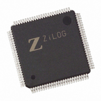
EZ80190AZ050EG Zilog, EZ80190AZ050EG Datasheet - Page 56

EZ80190AZ050EG
Manufacturer Part Number
EZ80190AZ050EG
Description
IC WEBSERVER 50MHZ XTEMP 100LQFP
Manufacturer
Zilog
Datasheet
1.EZ80190AZ050SG.pdf
(221 pages)
Specifications of EZ80190AZ050EG
Processor Type
eZ80
Features
High Speed, Single-Cycle Instruction-Fetch
Speed
50MHz
Voltage
3.3V
Mounting Type
Surface Mount
Package / Case
100-LQFP
Processor Series
EZ80190x
Core
eZ80
Data Bus Width
8 bit
Program Memory Type
ROMLess
Data Ram Size
8 KB
Interface Type
I2C, IrDA, SPI, UART
Maximum Clock Frequency
50 MHz
Number Of Programmable I/os
32
Number Of Timers
6
Operating Supply Voltage
3 V to 3.6 V
Maximum Operating Temperature
+ 70 C
Mounting Style
SMD/SMT
Minimum Operating Temperature
0 C
Lead Free Status / RoHS Status
Lead free / RoHS Compliant
Other names
269-3865
EZ80190AZ050EG
EZ80190AZ050EG
Available stocks
Company
Part Number
Manufacturer
Quantity
Price
Company:
Part Number:
EZ80190AZ050EG
Manufacturer:
TYCO
Quantity:
120
Company:
Part Number:
EZ80190AZ050EG
Manufacturer:
Zilog
Quantity:
70
- Current page: 56 of 221
- Download datasheet (4Mb)
GPIO Interrupts
PS006614-1208
System
DATA
Clock
Bus
Register (Output)
Level-Triggered Interrupts
GPIO Data
D
Q
Each port pin can be used as an interrupt source. Interrupts can be either level- or edge-
triggered.
When the port is configured for level-triggered interrupts, the corresponding port pin is
tristated. An interrupt request is generated when the level at the pin is the same as the level
stored in the Port x Data register. The port pin value is sampled by the system clock. The
input pin must be held at the selected interrupt level for a minimum of 2 clock periods to
initiate an interrupt. The interrupt request remains active as long as this condition is main-
tained at the external source.
For example, if PA3 is programmed for low-level interrupt and the pin is forced Low for 2
clock cycles, an interrupt request signal is generated from that port pin and sent to the
CPU. The interrupt request signal remains active until the external device driving PA3
Mode 1
Mode 4
Mode 1
Mode 3
System
Clock
Register (Input)
Figure 7. GPIO Port Pin Block Diagram
GPIO Data
Q
D
Q
D
GND
VDD
General-Purpose Input/Output
Product Specification
Port
Pin
eZ80190
46
Related parts for EZ80190AZ050EG
Image
Part Number
Description
Manufacturer
Datasheet
Request
R

Part Number:
Description:
Communication Controllers, ZILOG INTELLIGENT PERIPHERAL CONTROLLER (ZIP)
Manufacturer:
Zilog, Inc.
Datasheet:

Part Number:
Description:
KIT DEV FOR Z8 ENCORE 16K TO 64K
Manufacturer:
Zilog
Datasheet:

Part Number:
Description:
KIT DEV Z8 ENCORE XP 28-PIN
Manufacturer:
Zilog
Datasheet:

Part Number:
Description:
DEV KIT FOR Z8 ENCORE 8K/4K
Manufacturer:
Zilog
Datasheet:

Part Number:
Description:
KIT DEV Z8 ENCORE XP 28-PIN
Manufacturer:
Zilog
Datasheet:

Part Number:
Description:
DEV KIT FOR Z8 ENCORE 4K TO 8K
Manufacturer:
Zilog
Datasheet:

Part Number:
Description:
CMOS Z8 microcontroller. ROM 16 Kbytes, RAM 256 bytes, speed 16 MHz, 32 lines I/O, 3.0V to 5.5V
Manufacturer:
Zilog, Inc.
Datasheet:

Part Number:
Description:
Low-cost microcontroller. 512 bytes ROM, 61 bytes RAM, 8 MHz
Manufacturer:
Zilog, Inc.
Datasheet:

Part Number:
Description:
Z8 4K OTP Microcontroller
Manufacturer:
Zilog, Inc.
Datasheet:

Part Number:
Description:
CMOS SUPER8 ROMLESS MCU
Manufacturer:
Zilog, Inc.
Datasheet:

Part Number:
Description:
SL1866 CMOSZ8 OTP Microcontroller
Manufacturer:
Zilog, Inc.
Datasheet:

Part Number:
Description:
SL1866 CMOSZ8 OTP Microcontroller
Manufacturer:
Zilog, Inc.
Datasheet:

Part Number:
Description:
OTP (KB) = 1, RAM = 125, Speed = 12, I/O = 14, 8-bit Timers = 2, Comm Interfaces Other Features = Por, LV Protect, Voltage = 4.5-5.5V
Manufacturer:
Zilog, Inc.
Datasheet:

Part Number:
Description:
Manufacturer:
Zilog, Inc.
Datasheet:


