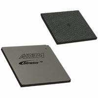
EP1S40B956C5 Altera, EP1S40B956C5 Datasheet - Page 287

EP1S40B956C5
Manufacturer Part Number
EP1S40B956C5
Description
IC STRATIX FPGA 40K LE 956-BGA
Manufacturer
Altera
Series
Stratix®r
Datasheet
1.EP1S10F484I6N.pdf
(864 pages)
Specifications of EP1S40B956C5
Number Of Logic Elements/cells
41250
Number Of Labs/clbs
4125
Total Ram Bits
3423744
Number Of I /o
683
Voltage - Supply
1.425 V ~ 1.575 V
Mounting Type
Surface Mount
Operating Temperature
0°C ~ 85°C
Package / Case
956-BGA
Lead Free Status / RoHS Status
Contains lead / RoHS non-compliant
Number Of Gates
-
Available stocks
Company
Part Number
Manufacturer
Quantity
Price
Part Number:
EP1S40B956C5
Manufacturer:
ALTERA/阿尔特拉
Quantity:
20 000
- Current page: 287 of 864
- Download datasheet (11Mb)
A
Accumulator
Adder/Output Blocks
Adder/Subtractor
AGP 1x Specifications
AGP 2x Specifications
Architecture
Altera Corporation
Accumulator
36 x 36 Multiply Mode
addnsub Signal
Block Diagram
Bus Hold
Byte Alignment
Carry-Select Chain
Clear & Preset Logic Control
Combined Resources
Dedicated Circuitry
Device Resources
Device Routing Scheme
Digital Signal Processing Block
Direct Link Connection
Dynamic Arithmetic Mode
Four-Multipliers
Functional Description
LAB
LE Operating Modes
Logic Elements
Modes of Operation
Multiplier Size & Configurations per DSP
Multiply-Accumulator Mode
MultiTrack Interconnect
Normal Mode
2–63
in LE
Adder Mode
Interconnects
Logic Array Blocks
Structure
in LE
2–63
block
2–11
2–9
2–121
2–1
2–63
2–70
2–4
2–9
2–2
2–6
2–8
2–140
2–68
2–4
2–3
2–11
4–13
4–13
2–61
2–137
2–64
2–8
2–78
2–3
2–66
2–1
2–5
2–20
2–14
2–10
2–13
2–67
2–52
C
Class I Specifications 4–11,
Class II Specifications 4–11, 4–12,
Clocks
Open-Drain Output
Power Sequencing & Hot Socketing
Programmable Drive Strength
Programmable Pull-Up Resistor
Simple Multiplier Mode
Single-Port Mode
Slew-Rate Control
Two-Multipliers
Clock Feedback
Clock Multiplication & Division 2–88,
Clock Switchover
Delay
EP1S10, EP1S20 & EP1S25
EP1S25, EP1S20 & EP1S10 Device Fast Clock
EP1S30 Device Fast Regional Clock Pin Con-
EP1S30, EP1S40, EP1S60, EP1S80
External Clock
Fast Regional Clock External I/O Timing
Fast Regional Clock Network
Adder Mode
Adder Mode Implementing Complex
Device I/O Clock Groups
Device I/O Clock Groups
Inputs
Outputs 2–92,
Outputs for Enhanced PLLs 11 & 12
Outputs for PLLs 5 & 6
2–88
Pin Connections to Fast Regional
Clocks
nections to Fast Regional Clocks
Parameters
2–97
Multiply
2–102
2–80
2–81
2–77
2–96
2–67
2–103
4–34
2–51
2–68
2–120
2–120
4–12
2–64
2–93
2–76
Index
4–13
2–119
2–122
Index–1
2–140
2–101
2–78
2–95
Related parts for EP1S40B956C5
Image
Part Number
Description
Manufacturer
Datasheet
Request
R

Part Number:
Description:
CYCLONE II STARTER KIT EP2C20N
Manufacturer:
Altera
Datasheet:

Part Number:
Description:
CPLD, EP610 Family, ECMOS Process, 300 Gates, 16 Macro Cells, 16 Reg., 16 User I/Os, 5V Supply, 35 Speed Grade, 24DIP
Manufacturer:
Altera Corporation
Datasheet:

Part Number:
Description:
CPLD, EP610 Family, ECMOS Process, 300 Gates, 16 Macro Cells, 16 Reg., 16 User I/Os, 5V Supply, 15 Speed Grade, 24DIP
Manufacturer:
Altera Corporation
Datasheet:

Part Number:
Description:
Manufacturer:
Altera Corporation
Datasheet:

Part Number:
Description:
CPLD, EP610 Family, ECMOS Process, 300 Gates, 16 Macro Cells, 16 Reg., 16 User I/Os, 5V Supply, 30 Speed Grade, 24DIP
Manufacturer:
Altera Corporation
Datasheet:

Part Number:
Description:
High-performance, low-power erasable programmable logic devices with 8 macrocells, 10ns
Manufacturer:
Altera Corporation
Datasheet:

Part Number:
Description:
High-performance, low-power erasable programmable logic devices with 8 macrocells, 7ns
Manufacturer:
Altera Corporation
Datasheet:

Part Number:
Description:
Classic EPLD
Manufacturer:
Altera Corporation
Datasheet:

Part Number:
Description:
High-performance, low-power erasable programmable logic devices with 8 macrocells, 10ns
Manufacturer:
Altera Corporation
Datasheet:

Part Number:
Description:
Manufacturer:
Altera Corporation
Datasheet:

Part Number:
Description:
Manufacturer:
Altera Corporation
Datasheet:

Part Number:
Description:
Manufacturer:
Altera Corporation
Datasheet:

Part Number:
Description:
CPLD, EP610 Family, ECMOS Process, 300 Gates, 16 Macro Cells, 16 Reg., 16 User I/Os, 5V Supply, 25 Speed Grade, 24DIP
Manufacturer:
Altera Corporation
Datasheet:


