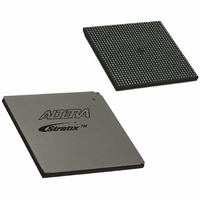
EP1S40B956C5 Altera, EP1S40B956C5 Datasheet - Page 46

EP1S40B956C5
Manufacturer Part Number
EP1S40B956C5
Description
IC STRATIX FPGA 40K LE 956-BGA
Manufacturer
Altera
Series
Stratix®r
Datasheet
1.EP1S10F484I6N.pdf
(864 pages)
Specifications of EP1S40B956C5
Number Of Logic Elements/cells
41250
Number Of Labs/clbs
4125
Total Ram Bits
3423744
Number Of I /o
683
Voltage - Supply
1.425 V ~ 1.575 V
Mounting Type
Surface Mount
Operating Temperature
0°C ~ 85°C
Package / Case
956-BGA
Lead Free Status / RoHS Status
Contains lead / RoHS non-compliant
Number Of Gates
-
Available stocks
Company
Part Number
Manufacturer
Quantity
Price
Part Number:
EP1S40B956C5
Manufacturer:
ALTERA/阿尔特拉
Quantity:
20 000
- Current page: 46 of 864
- Download datasheet (11Mb)
TriMatrix Memory
2–22
Stratix Device Handbook, Volume 1
1
Memory Modes
TriMatrix memory blocks include input registers that synchronize writes
and output registers to pipeline designs and improve system
performance. M4K and M-RAM memory blocks offer a true dual-port
mode to support any combination of two-port operations: two reads, two
writes, or one read and one write at two different clock frequencies.
Figure 2–12
Figure 2–12. True Dual-Port Memory Configuration
Notes to
(1)
(2)
Configurations
Table 2–3. TriMatrix Memory Features (Part 2 of 2)
Memory Feature
See
The M-RAM block does not support memory initializations. However, the
M-RAM block can emulate a ROM function using a dual-port RAM bock. The
Stratix device must write to the dual-port memory once and then disable the
write-enable ports afterwards.
Table 4–36
Table
Violating the setup or hold time on the address registers could
corrupt the memory contents. This applies to both read and
write operations.
shows true dual-port memory.
2–3:
for maximum performance information.
data
address
wren
clocken
q
aclr
A
clock
[ ]
512
256
128
64
64
32
32
A
M512 RAM Block
A
A
[ ]
(32 × 18 Bits)
A
A
A
[ ]
A
8
9
16
18
2
4
1
4K
2K
1K
512
512
256
256
128
128
M4K RAM Block
(128 × 36 Bits)
B
address
1
2
4
8
9
16
18
32
36
clocken
clock
data
wren
aclr
q
B
B
B
B
[ ]
[ ]
[ ]
B
B
B
Altera Corporation
64K
64K
32K
32K
16K
16K
8K
8K
4K
4K
(4K × 144 Bits)
M-RAM Block
64
72
128
144
8
9
16
18
32
36
July 2005
Related parts for EP1S40B956C5
Image
Part Number
Description
Manufacturer
Datasheet
Request
R

Part Number:
Description:
CYCLONE II STARTER KIT EP2C20N
Manufacturer:
Altera
Datasheet:

Part Number:
Description:
CPLD, EP610 Family, ECMOS Process, 300 Gates, 16 Macro Cells, 16 Reg., 16 User I/Os, 5V Supply, 35 Speed Grade, 24DIP
Manufacturer:
Altera Corporation
Datasheet:

Part Number:
Description:
CPLD, EP610 Family, ECMOS Process, 300 Gates, 16 Macro Cells, 16 Reg., 16 User I/Os, 5V Supply, 15 Speed Grade, 24DIP
Manufacturer:
Altera Corporation
Datasheet:

Part Number:
Description:
Manufacturer:
Altera Corporation
Datasheet:

Part Number:
Description:
CPLD, EP610 Family, ECMOS Process, 300 Gates, 16 Macro Cells, 16 Reg., 16 User I/Os, 5V Supply, 30 Speed Grade, 24DIP
Manufacturer:
Altera Corporation
Datasheet:

Part Number:
Description:
High-performance, low-power erasable programmable logic devices with 8 macrocells, 10ns
Manufacturer:
Altera Corporation
Datasheet:

Part Number:
Description:
High-performance, low-power erasable programmable logic devices with 8 macrocells, 7ns
Manufacturer:
Altera Corporation
Datasheet:

Part Number:
Description:
Classic EPLD
Manufacturer:
Altera Corporation
Datasheet:

Part Number:
Description:
High-performance, low-power erasable programmable logic devices with 8 macrocells, 10ns
Manufacturer:
Altera Corporation
Datasheet:

Part Number:
Description:
Manufacturer:
Altera Corporation
Datasheet:

Part Number:
Description:
Manufacturer:
Altera Corporation
Datasheet:

Part Number:
Description:
Manufacturer:
Altera Corporation
Datasheet:

Part Number:
Description:
CPLD, EP610 Family, ECMOS Process, 300 Gates, 16 Macro Cells, 16 Reg., 16 User I/Os, 5V Supply, 25 Speed Grade, 24DIP
Manufacturer:
Altera Corporation
Datasheet:


