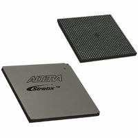
EP1S40B956C5 Altera, EP1S40B956C5 Datasheet - Page 813

EP1S40B956C5
Manufacturer Part Number
EP1S40B956C5
Description
IC STRATIX FPGA 40K LE 956-BGA
Manufacturer
Altera
Series
Stratix®r
Datasheet
1.EP1S10F484I6N.pdf
(864 pages)
Specifications of EP1S40B956C5
Number Of Logic Elements/cells
41250
Number Of Labs/clbs
4125
Total Ram Bits
3423744
Number Of I /o
683
Voltage - Supply
1.425 V ~ 1.575 V
Mounting Type
Surface Mount
Operating Temperature
0°C ~ 85°C
Package / Case
956-BGA
Lead Free Status / RoHS Status
Contains lead / RoHS non-compliant
Number Of Gates
-
Available stocks
Company
Part Number
Manufacturer
Quantity
Price
Part Number:
EP1S40B956C5
Manufacturer:
ALTERA/阿尔特拉
Quantity:
20 000
- Current page: 813 of 864
- Download datasheet (11Mb)
Altera Corporation
September 2004
f
A sample memory map output file for the preceding setup is shown
below. Notice all configuration pages are packed such that two pages can
share a flash data sector. This disallows partial programming of
application configurations in auto addressing mode.
See the Sharp LHF16J06 Data Sheet Flash memory used in EPC16 devices at
www.altera.com to correlate memory addresses to the EPC16 flash
sectors.
The block addressing mode allows better control of flash memory
allocation. You can allocate a specific flash memory region for each
application configuration page. This allocation is done by specifying a
block starting and block ending address. While selecting the size of the
region, you should account for growth in compressed configuration
bitstream sizes due to design changes and additions. In remote update
mode, all configuration data is top justified within this allotted memory.
In other words, the last byte of configuration data is stored such that it
coincides with the highest byte address location within the allotted space.
Lower unused memory address locations within the allotted region are
filled with 1's. These filler bits are transmitted during the application
configuration cycle, but are ignored by the Stratix device. The memory
map output file provides the exact byte address where real application
configuration data for each page begins. Note that any partial update of
the most recent application configuration should erase all allotted flash
sectors for that page before storing new configuration data.
In the block addressing mode, HEX input files can be optionally added to
the bottom boot and main flash data areas (one HEX file per area is
allowed). The HEX file can be stored with relative addressing or absolute
addressing. For more information on relative and absolute addressing,
see the Enhanced Configuration Devices (EPC4, EPC8 & EPC16) Data Sheet
chapter of the Configuration Handbook, Volume 2.
Figures 12–20
initial programming file with block addressing for remote update mode.
This example also illustrates preloading user HEX data into bottom boot
and main flash sectors.
1.
OPTION BITS
PAGE 0
PAGE 1
PAGE 2
Open the Convert Programming Files window from the File menu.
Block
Remote System Configuration with Stratix & Stratix GX Devices
and 12–21, and the following steps illustrate generating an
0x00010000
0x00010040
0x00054EFC
0x00099DB8
Start Address
Stratix Device Handbook, Volume 2
0x0001003F
0x00054EFA
0x00099DB6
0x000DEC72
End Address
12–35
Related parts for EP1S40B956C5
Image
Part Number
Description
Manufacturer
Datasheet
Request
R

Part Number:
Description:
CYCLONE II STARTER KIT EP2C20N
Manufacturer:
Altera
Datasheet:

Part Number:
Description:
CPLD, EP610 Family, ECMOS Process, 300 Gates, 16 Macro Cells, 16 Reg., 16 User I/Os, 5V Supply, 35 Speed Grade, 24DIP
Manufacturer:
Altera Corporation
Datasheet:

Part Number:
Description:
CPLD, EP610 Family, ECMOS Process, 300 Gates, 16 Macro Cells, 16 Reg., 16 User I/Os, 5V Supply, 15 Speed Grade, 24DIP
Manufacturer:
Altera Corporation
Datasheet:

Part Number:
Description:
Manufacturer:
Altera Corporation
Datasheet:

Part Number:
Description:
CPLD, EP610 Family, ECMOS Process, 300 Gates, 16 Macro Cells, 16 Reg., 16 User I/Os, 5V Supply, 30 Speed Grade, 24DIP
Manufacturer:
Altera Corporation
Datasheet:

Part Number:
Description:
High-performance, low-power erasable programmable logic devices with 8 macrocells, 10ns
Manufacturer:
Altera Corporation
Datasheet:

Part Number:
Description:
High-performance, low-power erasable programmable logic devices with 8 macrocells, 7ns
Manufacturer:
Altera Corporation
Datasheet:

Part Number:
Description:
Classic EPLD
Manufacturer:
Altera Corporation
Datasheet:

Part Number:
Description:
High-performance, low-power erasable programmable logic devices with 8 macrocells, 10ns
Manufacturer:
Altera Corporation
Datasheet:

Part Number:
Description:
Manufacturer:
Altera Corporation
Datasheet:

Part Number:
Description:
Manufacturer:
Altera Corporation
Datasheet:

Part Number:
Description:
Manufacturer:
Altera Corporation
Datasheet:

Part Number:
Description:
CPLD, EP610 Family, ECMOS Process, 300 Gates, 16 Macro Cells, 16 Reg., 16 User I/Os, 5V Supply, 25 Speed Grade, 24DIP
Manufacturer:
Altera Corporation
Datasheet:


