EP1S40B956C5 Altera, EP1S40B956C5 Datasheet - Page 749
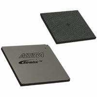
EP1S40B956C5
Manufacturer Part Number
EP1S40B956C5
Description
IC STRATIX FPGA 40K LE 956-BGA
Manufacturer
Altera
Series
Stratix®r
Datasheet
1.EP1S10F484I6N.pdf
(864 pages)
Specifications of EP1S40B956C5
Number Of Logic Elements/cells
41250
Number Of Labs/clbs
4125
Total Ram Bits
3423744
Number Of I /o
683
Voltage - Supply
1.425 V ~ 1.575 V
Mounting Type
Surface Mount
Operating Temperature
0°C ~ 85°C
Package / Case
956-BGA
Lead Free Status / RoHS Status
Contains lead / RoHS non-compliant
Number Of Gates
-
Available stocks
Company
Part Number
Manufacturer
Quantity
Price

Part Number:
EP1S40B956C5
Manufacturer:
ALTERA/阿尔特拉
Quantity:
20 000


Figure 11–16. PPA Configuration Circuit
Note to
(1)
Altera Corporation
July 2005
The pull-up resistor should be connected to the same supply voltage as the Stratix or Stratix GX device.
Figure
ADDR
Address Decoder
11–16:
ADDR DATA[7..0]
Memory
Microprocessor
Figure 11–16
decoder controls the device’s nCS and CS pins. This decoder allows the
microprocessor to select the Stratix or Stratix GX device by accessing a
particular address, simplifying the configuration process.
The device’s nCS or CS pins can be toggled during PPA configuration if
the design meets the specifications for t
Table 11–10 on page
the nCS and CS signals. You can tie one of the nCS or CS signals to its
active state (i.e., nCS may be tied low) and toggle the other signal to
control configuration.
Stratix and Stratix GX devices can serialize data internally without the
microprocessor. When the Stratix or Stratix GX device is ready for the
next byte of configuration data, it drives RDYnBSY high. If the
microprocessor senses a high signal when it polls RDYnBSY, the
microprocessor strobes the next byte of configuration data into the
device. Alternatively, the nRS signal can be strobed, causing the
RDYnBSY signal to appear on DATA7. Because RDYnBSY does not need to
10 kΩ
V
CC
(1)
shows the PPA configuration circuit. An optional address
10 kΩ
11–36. The microprocessor can also directly control
V
CC
V
GND
(1)
CC
10 k Ω
(1)
nCS
CS
CONF_DONE
nSTATUS
nCE
DATA[7..0]
nWS
nRS
nCONFIG
RDYnBSY
Configuring Stratix & Stratix GX Devices
Stratix Device
Stratix Device Handbook, Volume 2
CSSU
, t
WSP
nCEO
MSEL2
MSEL1
MSEL0
DCLK
, and t
CSH
N.C.
V
CC
GND
given in
(1)
10 kΩ
V
CC
11–31
Related parts for EP1S40B956C5
Image
Part Number
Description
Manufacturer
Datasheet
Request
R

Part Number:
Description:
CYCLONE II STARTER KIT EP2C20N
Manufacturer:
Altera
Datasheet:


Part Number:
Description:
CPLD, EP610 Family, ECMOS Process, 300 Gates, 16 Macro Cells, 16 Reg., 16 User I/Os, 5V Supply, 35 Speed Grade, 24DIP
Manufacturer:
Altera Corporation
Datasheet:
Part Number:
Description:
CPLD, EP610 Family, ECMOS Process, 300 Gates, 16 Macro Cells, 16 Reg., 16 User I/Os, 5V Supply, 15 Speed Grade, 24DIP
Manufacturer:
Altera Corporation
Datasheet:
Part Number:
Description:
Manufacturer:
Altera Corporation
Datasheet:
Part Number:
Description:
CPLD, EP610 Family, ECMOS Process, 300 Gates, 16 Macro Cells, 16 Reg., 16 User I/Os, 5V Supply, 30 Speed Grade, 24DIP
Manufacturer:
Altera Corporation
Datasheet:
Part Number:
Description:
High-performance, low-power erasable programmable logic devices with 8 macrocells, 10ns
Manufacturer:
Altera Corporation
Datasheet:
Part Number:
Description:
High-performance, low-power erasable programmable logic devices with 8 macrocells, 7ns
Manufacturer:
Altera Corporation
Datasheet:
Part Number:
Description:
Classic EPLD
Manufacturer:
Altera Corporation
Datasheet:
Part Number:
Description:
High-performance, low-power erasable programmable logic devices with 8 macrocells, 10ns
Manufacturer:
Altera Corporation
Datasheet:
Part Number:
Description:
Manufacturer:
Altera Corporation
Datasheet:
Part Number:
Description:
Manufacturer:
Altera Corporation
Datasheet:
Part Number:
Description:
Manufacturer:
Altera Corporation
Datasheet:
Part Number:
Description:
CPLD, EP610 Family, ECMOS Process, 300 Gates, 16 Macro Cells, 16 Reg., 16 User I/Os, 5V Supply, 25 Speed Grade, 24DIP
Manufacturer:
Altera Corporation
Datasheet: