EP1S40B956C5 Altera, EP1S40B956C5 Datasheet - Page 295
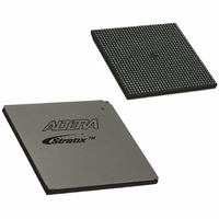
EP1S40B956C5
Manufacturer Part Number
EP1S40B956C5
Description
IC STRATIX FPGA 40K LE 956-BGA
Manufacturer
Altera
Series
Stratix®r
Datasheet
1.EP1S10F484I6N.pdf
(864 pages)
Specifications of EP1S40B956C5
Number Of Logic Elements/cells
41250
Number Of Labs/clbs
4125
Total Ram Bits
3423744
Number Of I /o
683
Voltage - Supply
1.425 V ~ 1.575 V
Mounting Type
Surface Mount
Operating Temperature
0°C ~ 85°C
Package / Case
956-BGA
Lead Free Status / RoHS Status
Contains lead / RoHS non-compliant
Number Of Gates
-
Available stocks
Company
Part Number
Manufacturer
Quantity
Price

Part Number:
EP1S40B956C5
Manufacturer:
ALTERA/阿尔特拉
Quantity:
20 000


Chapter Revision Dates ......................................................................... xiii
About This Handbook ............................................................................. xv
Section I. Clock Management
Chapter 1. General-Purpose PLLs in Stratix & Stratix GX Devices
Altera Corporation
How to Find Information ...................................................................................................................... xv
How to Contact Altera ........................................................................................................................... xv
Typographic Conventions .................................................................................................................... xvi
Revision History ....................................................................................................................... Section I–1
Introduction ............................................................................................................................................ 1–1
Enhanced PLLs ....................................................................................................................................... 1–5
Fast PLLs ............................................................................................................................................... 1–31
Clocking ................................................................................................................................................ 1–39
Board Layout ........................................................................................................................................ 1–50
Clock Multiplication & Division .................................................................................................... 1–9
External Clock Outputs ................................................................................................................. 1–10
Clock Feedback ............................................................................................................................... 1–14
Phase Shifting ................................................................................................................................. 1–14
Lock Detect ...................................................................................................................................... 1–15
Programmable Duty Cycle ........................................................................................................... 1–16
General Advanced Clear & Enable Control ............................................................................... 1–16
Programmable Bandwidth ............................................................................................................ 1–18
Clock Switchover ............................................................................................................................ 1–25
Spread-Spectrum Clocking ........................................................................................................... 1–25
PLL Reconfiguration ...................................................................................................................... 1–30
Enhanced PLL Pins ........................................................................................................................ 1–30
Clock Multiplication & Division .................................................................................................. 1–34
External Clock Outputs ................................................................................................................. 1–34
Phase Shifting ................................................................................................................................. 1–35
Programmable Duty Cycle ........................................................................................................... 1–36
Control Signals ................................................................................................................................ 1–36
Pins ................................................................................................................................................... 1–37
Global & Hierarchical Clocking ................................................................................................... 1–39
Clock Input Connections ............................................................................................................... 1–41
Clock Output Connections ............................................................................................................ 1–43
VCCA & GNDA ............................................................................................................................. 1–50
Contents
iii
Related parts for EP1S40B956C5
Image
Part Number
Description
Manufacturer
Datasheet
Request
R

Part Number:
Description:
CYCLONE II STARTER KIT EP2C20N
Manufacturer:
Altera
Datasheet:


Part Number:
Description:
CPLD, EP610 Family, ECMOS Process, 300 Gates, 16 Macro Cells, 16 Reg., 16 User I/Os, 5V Supply, 35 Speed Grade, 24DIP
Manufacturer:
Altera Corporation
Datasheet:
Part Number:
Description:
CPLD, EP610 Family, ECMOS Process, 300 Gates, 16 Macro Cells, 16 Reg., 16 User I/Os, 5V Supply, 15 Speed Grade, 24DIP
Manufacturer:
Altera Corporation
Datasheet:
Part Number:
Description:
Manufacturer:
Altera Corporation
Datasheet:
Part Number:
Description:
CPLD, EP610 Family, ECMOS Process, 300 Gates, 16 Macro Cells, 16 Reg., 16 User I/Os, 5V Supply, 30 Speed Grade, 24DIP
Manufacturer:
Altera Corporation
Datasheet:
Part Number:
Description:
High-performance, low-power erasable programmable logic devices with 8 macrocells, 10ns
Manufacturer:
Altera Corporation
Datasheet:
Part Number:
Description:
High-performance, low-power erasable programmable logic devices with 8 macrocells, 7ns
Manufacturer:
Altera Corporation
Datasheet:
Part Number:
Description:
Classic EPLD
Manufacturer:
Altera Corporation
Datasheet:
Part Number:
Description:
High-performance, low-power erasable programmable logic devices with 8 macrocells, 10ns
Manufacturer:
Altera Corporation
Datasheet:
Part Number:
Description:
Manufacturer:
Altera Corporation
Datasheet:
Part Number:
Description:
Manufacturer:
Altera Corporation
Datasheet:
Part Number:
Description:
Manufacturer:
Altera Corporation
Datasheet:
Part Number:
Description:
CPLD, EP610 Family, ECMOS Process, 300 Gates, 16 Macro Cells, 16 Reg., 16 User I/Os, 5V Supply, 25 Speed Grade, 24DIP
Manufacturer:
Altera Corporation
Datasheet: