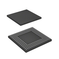
HD6417712BPV Renesas Electronics America, HD6417712BPV Datasheet - Page 121

HD6417712BPV
Manufacturer Part Number
HD6417712BPV
Description
MPU 1.5/3.3V 0K PB-FREE 256-BGA
Manufacturer
Renesas Electronics America
Series
SuperH® SH Ethernetr
Datasheet
1.HD6417712BPV.pdf
(980 pages)
Specifications of HD6417712BPV
Core Processor
SH-3 DSP
Core Size
32-Bit
Speed
200MHz
Connectivity
EBI/EMI, Ethernet, FIFO, SCI, SIO
Peripherals
DMA, POR, WDT
Number Of I /o
24
Program Memory Type
ROMless
Ram Size
16K x 8
Voltage - Supply (vcc/vdd)
1.4 V ~ 1.6 V
Oscillator Type
External
Operating Temperature
-20°C ~ 75°C
Package / Case
256-BGA
Lead Free Status / RoHS Status
Lead free / RoHS Compliant
Eeprom Size
-
Program Memory Size
-
Data Converters
-
Available stocks
Company
Part Number
Manufacturer
Quantity
Price
Company:
Part Number:
HD6417712BPV
Manufacturer:
Renesas Electronics America
Quantity:
10 000
- Current page: 121 of 980
- Download datasheet (6Mb)
Before entering the exception handling state, all bits including the DSP extension bits of the SR
registers are saved in the SSR. Before returning from the exception handling, all bits including the
DSP extension bits of the SR must be restored. If the repeat control must be recovered before
entering the exception handling state, the RS and RE registers must be recovered to the value that
existed before exception handling. In addition, if it is necessary to recover modulo control before
entering the exception handling state, the MOD register must be recovered to the value that
existed before exception handling.
3.2.4
The DSP unit incorporates eight data registers (A0, A1, X0, X1, Y0, Y1, M0, and M1) and a status
register (DSR). Figure 3.3 shows the DSP register configuration. These are 32-bit width registers
with the exception of registers A0 and A1. Registers A0 and A1 include 8 guard bits (fields A0G
and A1G), giving them a total width of 40 bits. The DSR register stores the DSP data operation
result (zero, negative, others). The DSP register has a DC bit whose function is similar to the T bit
of the CPU register. For details on DSR bits, refer to section 3.5, DSP Data Operation Instructions.
DSP Registers
31
39
....................................................
A0G
A1G
32 31
Figure 3.3 DSP Register Configuration
(a) DSP data registers
A0
A1
M0
M1
X0
X1
Y0
Y1
12 11
(b) DSP status register (DSR)
TS[2:0]
0
9
TC GT
8
Others: Undefined
7
DSR : All 0
Initial value
6
Z
Rev. 1.00 Dec. 27, 2005 Page 77 of 1044
N
5
4
V
3
CS[2:0]
Section 3 DSP Operating Unit
1
DC
0
REJ09B0269-0100
Related parts for HD6417712BPV
Image
Part Number
Description
Manufacturer
Datasheet
Request
R

Part Number:
Description:
KIT STARTER FOR M16C/29
Manufacturer:
Renesas Electronics America
Datasheet:

Part Number:
Description:
KIT STARTER FOR R8C/2D
Manufacturer:
Renesas Electronics America
Datasheet:

Part Number:
Description:
R0K33062P STARTER KIT
Manufacturer:
Renesas Electronics America
Datasheet:

Part Number:
Description:
KIT STARTER FOR R8C/23 E8A
Manufacturer:
Renesas Electronics America
Datasheet:

Part Number:
Description:
KIT STARTER FOR R8C/25
Manufacturer:
Renesas Electronics America
Datasheet:

Part Number:
Description:
KIT STARTER H8S2456 SHARPE DSPLY
Manufacturer:
Renesas Electronics America
Datasheet:

Part Number:
Description:
KIT STARTER FOR R8C38C
Manufacturer:
Renesas Electronics America
Datasheet:

Part Number:
Description:
KIT STARTER FOR R8C35C
Manufacturer:
Renesas Electronics America
Datasheet:

Part Number:
Description:
KIT STARTER FOR R8CL3AC+LCD APPS
Manufacturer:
Renesas Electronics America
Datasheet:

Part Number:
Description:
KIT STARTER FOR RX610
Manufacturer:
Renesas Electronics America
Datasheet:

Part Number:
Description:
KIT STARTER FOR R32C/118
Manufacturer:
Renesas Electronics America
Datasheet:

Part Number:
Description:
KIT DEV RSK-R8C/26-29
Manufacturer:
Renesas Electronics America
Datasheet:

Part Number:
Description:
KIT STARTER FOR SH7124
Manufacturer:
Renesas Electronics America
Datasheet:

Part Number:
Description:
KIT STARTER FOR H8SX/1622
Manufacturer:
Renesas Electronics America
Datasheet:

Part Number:
Description:
KIT DEV FOR SH7203
Manufacturer:
Renesas Electronics America
Datasheet:


