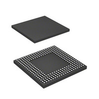
HD6417712BPV Renesas Electronics America, HD6417712BPV Datasheet - Page 618

HD6417712BPV
Manufacturer Part Number
HD6417712BPV
Description
MPU 1.5/3.3V 0K PB-FREE 256-BGA
Manufacturer
Renesas Electronics America
Series
SuperH® SH Ethernetr
Datasheet
1.HD6417712BPV.pdf
(980 pages)
Specifications of HD6417712BPV
Core Processor
SH-3 DSP
Core Size
32-Bit
Speed
200MHz
Connectivity
EBI/EMI, Ethernet, FIFO, SCI, SIO
Peripherals
DMA, POR, WDT
Number Of I /o
24
Program Memory Type
ROMless
Ram Size
16K x 8
Voltage - Supply (vcc/vdd)
1.4 V ~ 1.6 V
Oscillator Type
External
Operating Temperature
-20°C ~ 75°C
Package / Case
256-BGA
Lead Free Status / RoHS Status
Lead free / RoHS Compliant
Eeprom Size
-
Program Memory Size
-
Data Converters
-
Available stocks
Company
Part Number
Manufacturer
Quantity
Price
Company:
Part Number:
HD6417712BPV
Manufacturer:
Renesas Electronics America
Quantity:
10 000
- Current page: 618 of 980
- Download datasheet (6Mb)
Section 16 Serial Communication Interface with FIFO (SCIF)
Figure 16.12 shows a sample the SCIF initialization flowchart.
Rev. 1.00 Dec. 27, 2005 Page 574 of 932
REJ09B0269-0100
Set transmit or receive format in SCSMR
Read BRK, DR, and ER flags in SCFSR
Set external pins (SCIFnCK, TxD, RxD)
Set TFRST and RFRST bits in SCFCR
TTRG0 bits in SCFCR. Clear TFRST
Clear TE and RE bits in SCSCR to 0
Set CKE1 and CKE0 bits in SCSCR
Set TE and RE bits in SCSCR to 1
Set RTRG1, RTRG0, TTRG1, and
and set RIE, TIE, and REIE bits
and clear the flags by writing 0
(TE, RE, TIE, and RIE bits are
to 1 and clear buffer of FIFO
1-bit interval elapsed?
and RFRST bits to 0.
Set value in SCBRR
Start Initialization
cleared to 0)
End
Yes
Figure 16.12 Sample the SCIF Initialization Flowchart
Wait
No
1.
2.
3.
4.
5.
6.
Keep the TE and RE bits cleared to 0 until initialization
has been completed.
Set the CKE1 and CKE0 bits.
Set the transfer or receive format in SCSMR.
Write a value corresponding to the bit rate in SCBRR.
(Not necessary if an external clock is used.) After this
setting wait for at least 1-bit interval.
Set the external pins. Specifies the pins as RxD input
in reception and TxD output in transmission. Set the
SCIFnCK input/output according to the CKE1 and
CKE0 settings.
Set the TE bit or RE bit in SCSCR to 1. Also, set the
TIE, RIE, and REIE bits. At this time, the TxD, RxD,
and SCIFnCK pins can be used. In transmission, the
TxD pin is in the mark state. When reception in
clock synchronous mode and synchronous clock output
(clock master) are selected, a clock is output from the
SCIFnCK pin.
Related parts for HD6417712BPV
Image
Part Number
Description
Manufacturer
Datasheet
Request
R

Part Number:
Description:
KIT STARTER FOR M16C/29
Manufacturer:
Renesas Electronics America
Datasheet:

Part Number:
Description:
KIT STARTER FOR R8C/2D
Manufacturer:
Renesas Electronics America
Datasheet:

Part Number:
Description:
R0K33062P STARTER KIT
Manufacturer:
Renesas Electronics America
Datasheet:

Part Number:
Description:
KIT STARTER FOR R8C/23 E8A
Manufacturer:
Renesas Electronics America
Datasheet:

Part Number:
Description:
KIT STARTER FOR R8C/25
Manufacturer:
Renesas Electronics America
Datasheet:

Part Number:
Description:
KIT STARTER H8S2456 SHARPE DSPLY
Manufacturer:
Renesas Electronics America
Datasheet:

Part Number:
Description:
KIT STARTER FOR R8C38C
Manufacturer:
Renesas Electronics America
Datasheet:

Part Number:
Description:
KIT STARTER FOR R8C35C
Manufacturer:
Renesas Electronics America
Datasheet:

Part Number:
Description:
KIT STARTER FOR R8CL3AC+LCD APPS
Manufacturer:
Renesas Electronics America
Datasheet:

Part Number:
Description:
KIT STARTER FOR RX610
Manufacturer:
Renesas Electronics America
Datasheet:

Part Number:
Description:
KIT STARTER FOR R32C/118
Manufacturer:
Renesas Electronics America
Datasheet:

Part Number:
Description:
KIT DEV RSK-R8C/26-29
Manufacturer:
Renesas Electronics America
Datasheet:

Part Number:
Description:
KIT STARTER FOR SH7124
Manufacturer:
Renesas Electronics America
Datasheet:

Part Number:
Description:
KIT STARTER FOR H8SX/1622
Manufacturer:
Renesas Electronics America
Datasheet:

Part Number:
Description:
KIT DEV FOR SH7203
Manufacturer:
Renesas Electronics America
Datasheet:


