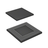
HD6417712BPV Renesas Electronics America, HD6417712BPV Datasheet - Page 465

HD6417712BPV
Manufacturer Part Number
HD6417712BPV
Description
MPU 1.5/3.3V 0K PB-FREE 256-BGA
Manufacturer
Renesas Electronics America
Series
SuperH® SH Ethernetr
Datasheet
1.HD6417712BPV.pdf
(980 pages)
Specifications of HD6417712BPV
Core Processor
SH-3 DSP
Core Size
32-Bit
Speed
200MHz
Connectivity
EBI/EMI, Ethernet, FIFO, SCI, SIO
Peripherals
DMA, POR, WDT
Number Of I /o
24
Program Memory Type
ROMless
Ram Size
16K x 8
Voltage - Supply (vcc/vdd)
1.4 V ~ 1.6 V
Oscillator Type
External
Operating Temperature
-20°C ~ 75°C
Package / Case
256-BGA
Lead Free Status / RoHS Status
Lead free / RoHS Compliant
Eeprom Size
-
Program Memory Size
-
Data Converters
-
Available stocks
Company
Part Number
Manufacturer
Quantity
Price
Company:
Part Number:
HD6417712BPV
Manufacturer:
Renesas Electronics America
Quantity:
10 000
- Current page: 465 of 980
- Download datasheet (6Mb)
Single Write: A write access ends in one cycle when data is written in non-cachable region and
the data bus width is larger than or equal to access size.
Figure 12.18 shows the single write basic timing.
Bank Active: The synchronous DRAM bank function is used to support high-speed accesses to
the same row address. When the BACTV bit in SDCR is 1, accesses are performed using
commands without auto-precharge (READ or WRIT). This function is called bank-active function.
This function is valid only for either the upper or lower bits of area 3. When area 3 is set to bank-
active mode, area 2 should be set to normal space or byte-selection SRAM. When areas 2 and 3
are both set to SDRAM, auto precharge mode must be set.
When a bank-active function is used, precharging is not performed when the access ends. When
accessing the same row address in the same bank, it is possible to issue the READ or WRIT
command immediately, without issuing an ACTV command. As synchronous DRAM is internally
divided into several banks, it is possible to activate one row address in each bank. If the next
access is to a different row address, a PRE command is first issued to precharge the relevant bank,
Figure 12.18 Basic Timing for Single Write (Auto-Precharge)
A12/A11*
Notes: 1. Address pin to be connected to the A10 pin of SDRAM.
D31 to D0
DACKn*
A25 to A0
RD/WR
DQMxx
CKIO
RAS
CAS
CSn
BS
2. The waveform for DACKn is when active low is specified.
1
2
Tr
Tc1
Trwl
Tap
Rev. 1.00 Dec. 27, 2005 Page 421 of 932
Section 12 Bus State Controller (BSC)
REJ09B0269-0100
Related parts for HD6417712BPV
Image
Part Number
Description
Manufacturer
Datasheet
Request
R

Part Number:
Description:
KIT STARTER FOR M16C/29
Manufacturer:
Renesas Electronics America
Datasheet:

Part Number:
Description:
KIT STARTER FOR R8C/2D
Manufacturer:
Renesas Electronics America
Datasheet:

Part Number:
Description:
R0K33062P STARTER KIT
Manufacturer:
Renesas Electronics America
Datasheet:

Part Number:
Description:
KIT STARTER FOR R8C/23 E8A
Manufacturer:
Renesas Electronics America
Datasheet:

Part Number:
Description:
KIT STARTER FOR R8C/25
Manufacturer:
Renesas Electronics America
Datasheet:

Part Number:
Description:
KIT STARTER H8S2456 SHARPE DSPLY
Manufacturer:
Renesas Electronics America
Datasheet:

Part Number:
Description:
KIT STARTER FOR R8C38C
Manufacturer:
Renesas Electronics America
Datasheet:

Part Number:
Description:
KIT STARTER FOR R8C35C
Manufacturer:
Renesas Electronics America
Datasheet:

Part Number:
Description:
KIT STARTER FOR R8CL3AC+LCD APPS
Manufacturer:
Renesas Electronics America
Datasheet:

Part Number:
Description:
KIT STARTER FOR RX610
Manufacturer:
Renesas Electronics America
Datasheet:

Part Number:
Description:
KIT STARTER FOR R32C/118
Manufacturer:
Renesas Electronics America
Datasheet:

Part Number:
Description:
KIT DEV RSK-R8C/26-29
Manufacturer:
Renesas Electronics America
Datasheet:

Part Number:
Description:
KIT STARTER FOR SH7124
Manufacturer:
Renesas Electronics America
Datasheet:

Part Number:
Description:
KIT STARTER FOR H8SX/1622
Manufacturer:
Renesas Electronics America
Datasheet:

Part Number:
Description:
KIT DEV FOR SH7203
Manufacturer:
Renesas Electronics America
Datasheet:


