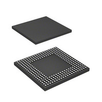
HD6417712BPV Renesas Electronics America, HD6417712BPV Datasheet - Page 42

HD6417712BPV
Manufacturer Part Number
HD6417712BPV
Description
MPU 1.5/3.3V 0K PB-FREE 256-BGA
Manufacturer
Renesas Electronics America
Series
SuperH® SH Ethernetr
Datasheet
1.HD6417712BPV.pdf
(980 pages)
Specifications of HD6417712BPV
Core Processor
SH-3 DSP
Core Size
32-Bit
Speed
200MHz
Connectivity
EBI/EMI, Ethernet, FIFO, SCI, SIO
Peripherals
DMA, POR, WDT
Number Of I /o
24
Program Memory Type
ROMless
Ram Size
16K x 8
Voltage - Supply (vcc/vdd)
1.4 V ~ 1.6 V
Oscillator Type
External
Operating Temperature
-20°C ~ 75°C
Package / Case
256-BGA
Lead Free Status / RoHS Status
Lead free / RoHS Compliant
Eeprom Size
-
Program Memory Size
-
Data Converters
-
Available stocks
Company
Part Number
Manufacturer
Quantity
Price
Company:
Part Number:
HD6417712BPV
Manufacturer:
Renesas Electronics America
Quantity:
10 000
- Current page: 42 of 980
- Download datasheet (6Mb)
Table 12.13
Table 12.13
Table 12.14
Table 12.15
Table 12.15
Table 12.16
Table 12.16
Table 12.17
Table 12.17
Table 12.18
Table 12.19
Table 12.20
Table 12.21
Section 13 Direct Memory Access Controller (DMAC)
Table 13.1
Table 13.2
Table 13.3
Table 13.4
Table 13.5
Table 13.6
Table 13.7
Table 13.8
Section 14 Timer Unit (TMU)
Table 14.1
Section 15 Realtime Clock (RTC)
Table 15.1
Table 15.2
Section 16 Serial Communication Interface with FIFO (SCIF)
Table 16.1
Rev. 1.00 Dec. 27, 2005 Page xl of xlii
Relationship between A2/3BSZ[1:0], A2/3ROW[1:0], A2/3COL[1:0], and
Address Multiplex Output (2)-1 ........................................................................... 405
Relationship between A2/3BSZ[1:0], A2/3ROW[1:0], A2/3COL[1:0], and
Address Multiplex Output (2)-2 ........................................................................... 406
Relationship between A2/3BSZ[1:0], A2/3ROW[1:0], A2/3COL[1:0], and
Address Multiplex Output (3)............................................................................... 408
Relationship between A2/3BSZ[1:0], A2/3ROW[1:0], A2/3COL[1:0], and
Address Multiplex Output (4)-1 ........................................................................... 409
Relationship between A2/3BSZ[1:0], A2/3ROW[1:0], A2/3COL[1:0], and
Address Multiplex Output (4)-2 ........................................................................... 410
Relationship between A2/3BSZ[1:0], A2/3ROW[1:0], A2/3COL[1:0], and
Address Multiplex Output (5)-1 ........................................................................... 411
Relationship between A2/3BSZ[1:0], A2/3ROW[1:0], A2/3COL[1:0], and
Address Multiplex Output (5)-2 ........................................................................... 412
Relationship between A2/3BSZ[1:0], A2/3ROW[1:0], A2/3COL[1:0], and
Address Multiplex Output (6)-1 ........................................................................... 413
Relationship between A2/3BSZ[1:0], A2/3ROW[1:0], A2/3COL[1:0], and
Address Multiplex Output (6)-2 ........................................................................... 414
Relationship between Access Size and Number of Bursts.................................... 415
Access Address in SDRAM Mode Register Write ............................................... 435
Output Addresses when EMRS Command is Issued ............................................ 438
Relationship between Bus Width, Access Size, and Number of Bursts................ 441
Pin Configuration.................................................................................................. 461
DMARS Setting.................................................................................................... 474
Selecting External Request Modes with RS Bits .................................................. 477
Selecting External Request Detection with DL, DS Bits ...................................... 478
Selecting External Request Detection with DO Bit .............................................. 478
Selecting On-Chip Peripheral Module Request Modes with RS3 to RS0 Bits ..... 479
Supported DMA Transfers.................................................................................... 482
Relationship of Request Modes and Bus Modes by DMA Transfer Category ..... 488
TMU Interrupt Sources......................................................................................... 504
Pin Configuration.................................................................................................. 507
Recommended Oscillator Circuit Constants (Recommended Values).................. 528
Pin Configuration.................................................................................................. 534
Related parts for HD6417712BPV
Image
Part Number
Description
Manufacturer
Datasheet
Request
R

Part Number:
Description:
KIT STARTER FOR M16C/29
Manufacturer:
Renesas Electronics America
Datasheet:

Part Number:
Description:
KIT STARTER FOR R8C/2D
Manufacturer:
Renesas Electronics America
Datasheet:

Part Number:
Description:
R0K33062P STARTER KIT
Manufacturer:
Renesas Electronics America
Datasheet:

Part Number:
Description:
KIT STARTER FOR R8C/23 E8A
Manufacturer:
Renesas Electronics America
Datasheet:

Part Number:
Description:
KIT STARTER FOR R8C/25
Manufacturer:
Renesas Electronics America
Datasheet:

Part Number:
Description:
KIT STARTER H8S2456 SHARPE DSPLY
Manufacturer:
Renesas Electronics America
Datasheet:

Part Number:
Description:
KIT STARTER FOR R8C38C
Manufacturer:
Renesas Electronics America
Datasheet:

Part Number:
Description:
KIT STARTER FOR R8C35C
Manufacturer:
Renesas Electronics America
Datasheet:

Part Number:
Description:
KIT STARTER FOR R8CL3AC+LCD APPS
Manufacturer:
Renesas Electronics America
Datasheet:

Part Number:
Description:
KIT STARTER FOR RX610
Manufacturer:
Renesas Electronics America
Datasheet:

Part Number:
Description:
KIT STARTER FOR R32C/118
Manufacturer:
Renesas Electronics America
Datasheet:

Part Number:
Description:
KIT DEV RSK-R8C/26-29
Manufacturer:
Renesas Electronics America
Datasheet:

Part Number:
Description:
KIT STARTER FOR SH7124
Manufacturer:
Renesas Electronics America
Datasheet:

Part Number:
Description:
KIT STARTER FOR H8SX/1622
Manufacturer:
Renesas Electronics America
Datasheet:

Part Number:
Description:
KIT DEV FOR SH7203
Manufacturer:
Renesas Electronics America
Datasheet:


