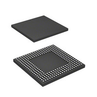
HD6417712BPV Renesas Electronics America, HD6417712BPV Datasheet - Page 486

HD6417712BPV
Manufacturer Part Number
HD6417712BPV
Description
MPU 1.5/3.3V 0K PB-FREE 256-BGA
Manufacturer
Renesas Electronics America
Series
SuperH® SH Ethernetr
Datasheet
1.HD6417712BPV.pdf
(980 pages)
Specifications of HD6417712BPV
Core Processor
SH-3 DSP
Core Size
32-Bit
Speed
200MHz
Connectivity
EBI/EMI, Ethernet, FIFO, SCI, SIO
Peripherals
DMA, POR, WDT
Number Of I /o
24
Program Memory Type
ROMless
Ram Size
16K x 8
Voltage - Supply (vcc/vdd)
1.4 V ~ 1.6 V
Oscillator Type
External
Operating Temperature
-20°C ~ 75°C
Package / Case
256-BGA
Lead Free Status / RoHS Status
Lead free / RoHS Compliant
Eeprom Size
-
Program Memory Size
-
Data Converters
-
Available stocks
Company
Part Number
Manufacturer
Quantity
Price
Company:
Part Number:
HD6417712BPV
Manufacturer:
Renesas Electronics America
Quantity:
10 000
- Current page: 486 of 980
- Download datasheet (6Mb)
Section 12 Bus State Controller (BSC)
12.5.7
The byte-selection SRAM interface is for access to an SRAM which has a byte-selection pin
(WEn (BEn)). This interface has 16-bit data pins and accesses SRAMs having upper and lower
byte selection pins, such as UB and LB.
When the BAS bit in CSnWCR is cleared to 0 (initial value), the write access timing of the byte-
selection SRAM interface is the same as that for the normal space interface. While in read access
of a byte-selection SRAM interface, the byte-selection signal is output from the WEn (BEn) pin,
which is different from that for the normal space interface. The basic access timing is shown in
figure 12.33. In write access, data is written to the memory according to the timing of the byte-
selection pin (WEn (BEn)). For details, refer to the data sheet for the corresponding memory.
If the BAS bit in CSnWCR is set to 1, the WEn (BEn) pin and RD/WR pin timings change. Figure
12.34 shows the basic access timing. In write access, data is written to the memory according to
the timing of the write enable pin (RD/WR). The data hold timing from RD/WR negation to data
write must be acquired by setting the HW[1:0] bits in CSnWCR. Figure 12.35 shows the access
timing when a software wait is specified.
Rev. 1.00 Dec. 27, 2005 Page 442 of 932
REJ09B0269-0100
Figure 12.32 Burst ROM (Clock Asynchronous) Access (Bus Width = 32 Bits,
Byte-Selection SRAM Interface
D31 to D0
A25 to A0
16-byte Transfer (Number of Bursts = 4), Access Wait for First Time = 2,
RD/WR
DACK
WAIT
CKIO
BS
RD
CS
T1
Access Wait for 2nd Time and after = 1)
Tw
Tw
TB2
Twb
TB2
Twb
TB2
Twb
T2
Related parts for HD6417712BPV
Image
Part Number
Description
Manufacturer
Datasheet
Request
R

Part Number:
Description:
KIT STARTER FOR M16C/29
Manufacturer:
Renesas Electronics America
Datasheet:

Part Number:
Description:
KIT STARTER FOR R8C/2D
Manufacturer:
Renesas Electronics America
Datasheet:

Part Number:
Description:
R0K33062P STARTER KIT
Manufacturer:
Renesas Electronics America
Datasheet:

Part Number:
Description:
KIT STARTER FOR R8C/23 E8A
Manufacturer:
Renesas Electronics America
Datasheet:

Part Number:
Description:
KIT STARTER FOR R8C/25
Manufacturer:
Renesas Electronics America
Datasheet:

Part Number:
Description:
KIT STARTER H8S2456 SHARPE DSPLY
Manufacturer:
Renesas Electronics America
Datasheet:

Part Number:
Description:
KIT STARTER FOR R8C38C
Manufacturer:
Renesas Electronics America
Datasheet:

Part Number:
Description:
KIT STARTER FOR R8C35C
Manufacturer:
Renesas Electronics America
Datasheet:

Part Number:
Description:
KIT STARTER FOR R8CL3AC+LCD APPS
Manufacturer:
Renesas Electronics America
Datasheet:

Part Number:
Description:
KIT STARTER FOR RX610
Manufacturer:
Renesas Electronics America
Datasheet:

Part Number:
Description:
KIT STARTER FOR R32C/118
Manufacturer:
Renesas Electronics America
Datasheet:

Part Number:
Description:
KIT DEV RSK-R8C/26-29
Manufacturer:
Renesas Electronics America
Datasheet:

Part Number:
Description:
KIT STARTER FOR SH7124
Manufacturer:
Renesas Electronics America
Datasheet:

Part Number:
Description:
KIT STARTER FOR H8SX/1622
Manufacturer:
Renesas Electronics America
Datasheet:

Part Number:
Description:
KIT DEV FOR SH7203
Manufacturer:
Renesas Electronics America
Datasheet:


