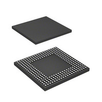
HD6417712BPV Renesas Electronics America, HD6417712BPV Datasheet - Page 616

HD6417712BPV
Manufacturer Part Number
HD6417712BPV
Description
MPU 1.5/3.3V 0K PB-FREE 256-BGA
Manufacturer
Renesas Electronics America
Series
SuperH® SH Ethernetr
Datasheet
1.HD6417712BPV.pdf
(980 pages)
Specifications of HD6417712BPV
Core Processor
SH-3 DSP
Core Size
32-Bit
Speed
200MHz
Connectivity
EBI/EMI, Ethernet, FIFO, SCI, SIO
Peripherals
DMA, POR, WDT
Number Of I /o
24
Program Memory Type
ROMless
Ram Size
16K x 8
Voltage - Supply (vcc/vdd)
1.4 V ~ 1.6 V
Oscillator Type
External
Operating Temperature
-20°C ~ 75°C
Package / Case
256-BGA
Lead Free Status / RoHS Status
Lead free / RoHS Compliant
Eeprom Size
-
Program Memory Size
-
Data Converters
-
Available stocks
Company
Part Number
Manufacturer
Quantity
Price
Company:
Part Number:
HD6417712BPV
Manufacturer:
Renesas Electronics America
Quantity:
10 000
- Current page: 616 of 980
- Download datasheet (6Mb)
Section 16 Serial Communication Interface with FIFO (SCIF)
When using a modem function and the receive FIFO (SCFRDR) is at least the number of the RTS
output trigger, the RTS signal goes high.
Receive data
RxD
16.4.3
In clock synchronous mode, the SCIF transmits and receives data synchronizing with clock pulses.
This mode is suitable for high-speed serial communication. In the SCIF, the transmitter and
receiver are independent. Therefore, by sharing the same clock, full-duplex communication can be
performed. Figure 16.11 shows the general format of clock synchronous serial communication.
In clock synchronous serial communication, data on the communication line is output from one
fall of the serial clock to the next. Data is guaranteed valid at the rise of the serial clock.
In serial communication, each character is output starting with the LSB and ending with the MSB.
After the MSB is output, the communication line remains in the state of the MSB.
Rev. 1.00 Dec. 27, 2005 Page 572 of 932
REJ09B0269-0100
RTS
Serial clock
Serial data
Note: * High except in continuous transmission/reception
Serial Operation in Clock Synchronous Mode
Don’t care
Figure 16.11 Data Format in Clock Synchronous Communication
Start
bit
0
*
D0
RTS goes high when receive data is
at least number of RTS output trigger
D1
Bit 0
LSB
Figure 16.10 RTS Control Operation
Bit 1
D6
One unit of transfer data (character or frame)
D7
Bit 2
Parity
bit
0/1
Stop
bit
Bit 3
RTS goes low when receive data is
less than number of RTS output trigger
Bit 4
Bit 5
Bit 6
MSB
Bit 7
*
Don’t care
Related parts for HD6417712BPV
Image
Part Number
Description
Manufacturer
Datasheet
Request
R

Part Number:
Description:
KIT STARTER FOR M16C/29
Manufacturer:
Renesas Electronics America
Datasheet:

Part Number:
Description:
KIT STARTER FOR R8C/2D
Manufacturer:
Renesas Electronics America
Datasheet:

Part Number:
Description:
R0K33062P STARTER KIT
Manufacturer:
Renesas Electronics America
Datasheet:

Part Number:
Description:
KIT STARTER FOR R8C/23 E8A
Manufacturer:
Renesas Electronics America
Datasheet:

Part Number:
Description:
KIT STARTER FOR R8C/25
Manufacturer:
Renesas Electronics America
Datasheet:

Part Number:
Description:
KIT STARTER H8S2456 SHARPE DSPLY
Manufacturer:
Renesas Electronics America
Datasheet:

Part Number:
Description:
KIT STARTER FOR R8C38C
Manufacturer:
Renesas Electronics America
Datasheet:

Part Number:
Description:
KIT STARTER FOR R8C35C
Manufacturer:
Renesas Electronics America
Datasheet:

Part Number:
Description:
KIT STARTER FOR R8CL3AC+LCD APPS
Manufacturer:
Renesas Electronics America
Datasheet:

Part Number:
Description:
KIT STARTER FOR RX610
Manufacturer:
Renesas Electronics America
Datasheet:

Part Number:
Description:
KIT STARTER FOR R32C/118
Manufacturer:
Renesas Electronics America
Datasheet:

Part Number:
Description:
KIT DEV RSK-R8C/26-29
Manufacturer:
Renesas Electronics America
Datasheet:

Part Number:
Description:
KIT STARTER FOR SH7124
Manufacturer:
Renesas Electronics America
Datasheet:

Part Number:
Description:
KIT STARTER FOR H8SX/1622
Manufacturer:
Renesas Electronics America
Datasheet:

Part Number:
Description:
KIT DEV FOR SH7203
Manufacturer:
Renesas Electronics America
Datasheet:


