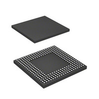
HD6417712BPV Renesas Electronics America, HD6417712BPV Datasheet - Page 497

HD6417712BPV
Manufacturer Part Number
HD6417712BPV
Description
MPU 1.5/3.3V 0K PB-FREE 256-BGA
Manufacturer
Renesas Electronics America
Series
SuperH® SH Ethernetr
Datasheet
1.HD6417712BPV.pdf
(980 pages)
Specifications of HD6417712BPV
Core Processor
SH-3 DSP
Core Size
32-Bit
Speed
200MHz
Connectivity
EBI/EMI, Ethernet, FIFO, SCI, SIO
Peripherals
DMA, POR, WDT
Number Of I /o
24
Program Memory Type
ROMless
Ram Size
16K x 8
Voltage - Supply (vcc/vdd)
1.4 V ~ 1.6 V
Oscillator Type
External
Operating Temperature
-20°C ~ 75°C
Package / Case
256-BGA
Lead Free Status / RoHS Status
Lead free / RoHS Compliant
Eeprom Size
-
Program Memory Size
-
Data Converters
-
Available stocks
Company
Part Number
Manufacturer
Quantity
Price
Company:
Part Number:
HD6417712BPV
Manufacturer:
Renesas Electronics America
Quantity:
10 000
- Current page: 497 of 980
- Download datasheet (6Mb)
12.5.9
The burst ROM (clock synchronous) interface is supported to access a ROM with a synchronous
burst function at high speed. The burst ROM interface accesses the burst ROM in the same way as
a normal space. This interface is valid only for area 0.
In the first access cycle, wait cycles are inserted. In this case, the number of wait cycles to be
inserted is specified by the W[3:0] bits of the CS0WCR. In the second and subsequent cycles, the
number of wait cycles to be inserted is specified by the BW[1:0] bits of the CS0WCR.
While the burst ROM is accessed (clock synchronous), the BS signal is asserted only for the first
access cycle and an external wait input is also valid for the first access cycle.
If the bus width is 16 bits, the burst length must be specified as 8. If the bus width is 32 bits, the
burst length must be specified as 4. The burst ROM interface does not support the 8-bit bus width
for the burst ROM. The burst ROM interface performs burst operations for all read accesses. For
example, in a longword access over a 16-bit bus, valid 16-bit data is read two times and invalid
16-bit data is read six times.
These invalid data read cycles increase the memory access time and degrade the program
execution speed and DMA transfer speed. To prevent this problem, a 16-byte read by cache fill or
16-byte read by the DMA should be used. The burst ROM interface performs write accesses in the
same way as normal space access.
Note: The burst ROM (clock synchronous) must be accessed as cacheable space.
D15 to D0
Address
DACKn*
RD/WR
WAIT
CKIO
CSn
RD
BS
Note: The waveform for DACKn is when active low is specified.
T1
Burst ROM (Clock Synchronous) Interface
Tw
Figure 12.45 Burst ROM (Clock Synchronous) Access Timing
Wait Cycles inserted in Second and Subsequent Accesses = 1)
(Burst Length = 8, Wait Cycles inserted in First Access = 2,
Tw
T2B
Twb
T2B
Twb
T2B
Twb
T2B
Twb
Rev. 1.00 Dec. 27, 2005 Page 453 of 932
T2B
Section 12 Bus State Controller (BSC)
Twb
T2B
Twb
T2B
REJ09B0269-0100
Twb
T2
Related parts for HD6417712BPV
Image
Part Number
Description
Manufacturer
Datasheet
Request
R

Part Number:
Description:
KIT STARTER FOR M16C/29
Manufacturer:
Renesas Electronics America
Datasheet:

Part Number:
Description:
KIT STARTER FOR R8C/2D
Manufacturer:
Renesas Electronics America
Datasheet:

Part Number:
Description:
R0K33062P STARTER KIT
Manufacturer:
Renesas Electronics America
Datasheet:

Part Number:
Description:
KIT STARTER FOR R8C/23 E8A
Manufacturer:
Renesas Electronics America
Datasheet:

Part Number:
Description:
KIT STARTER FOR R8C/25
Manufacturer:
Renesas Electronics America
Datasheet:

Part Number:
Description:
KIT STARTER H8S2456 SHARPE DSPLY
Manufacturer:
Renesas Electronics America
Datasheet:

Part Number:
Description:
KIT STARTER FOR R8C38C
Manufacturer:
Renesas Electronics America
Datasheet:

Part Number:
Description:
KIT STARTER FOR R8C35C
Manufacturer:
Renesas Electronics America
Datasheet:

Part Number:
Description:
KIT STARTER FOR R8CL3AC+LCD APPS
Manufacturer:
Renesas Electronics America
Datasheet:

Part Number:
Description:
KIT STARTER FOR RX610
Manufacturer:
Renesas Electronics America
Datasheet:

Part Number:
Description:
KIT STARTER FOR R32C/118
Manufacturer:
Renesas Electronics America
Datasheet:

Part Number:
Description:
KIT DEV RSK-R8C/26-29
Manufacturer:
Renesas Electronics America
Datasheet:

Part Number:
Description:
KIT STARTER FOR SH7124
Manufacturer:
Renesas Electronics America
Datasheet:

Part Number:
Description:
KIT STARTER FOR H8SX/1622
Manufacturer:
Renesas Electronics America
Datasheet:

Part Number:
Description:
KIT DEV FOR SH7203
Manufacturer:
Renesas Electronics America
Datasheet:


