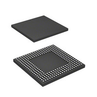
HD6417712BPV Renesas Electronics America, HD6417712BPV Datasheet - Page 281

HD6417712BPV
Manufacturer Part Number
HD6417712BPV
Description
MPU 1.5/3.3V 0K PB-FREE 256-BGA
Manufacturer
Renesas Electronics America
Series
SuperH® SH Ethernetr
Datasheet
1.HD6417712BPV.pdf
(980 pages)
Specifications of HD6417712BPV
Core Processor
SH-3 DSP
Core Size
32-Bit
Speed
200MHz
Connectivity
EBI/EMI, Ethernet, FIFO, SCI, SIO
Peripherals
DMA, POR, WDT
Number Of I /o
24
Program Memory Type
ROMless
Ram Size
16K x 8
Voltage - Supply (vcc/vdd)
1.4 V ~ 1.6 V
Oscillator Type
External
Operating Temperature
-20°C ~ 75°C
Package / Case
256-BGA
Lead Free Status / RoHS Status
Lead free / RoHS Compliant
Eeprom Size
-
Program Memory Size
-
Data Converters
-
Available stocks
Company
Part Number
Manufacturer
Quantity
Price
Company:
Part Number:
HD6417712BPV
Manufacturer:
Renesas Electronics America
Quantity:
10 000
- Current page: 281 of 980
- Download datasheet (6Mb)
8.2
Table 8.1 shows the INTC pin configuration.
Table 8.1
Notes: 1. The IRL3 to IRL0 pins and the IRQ3 to IRQ0 cannot be used simultaneously because
8.3
There are four types of interrupt sources: NMI, IRQ, IRL, and on-chip peripheral modules. Each
interrupt has a priority level (0 to 16), with 1 the lowest and 16 the highest. Priority level 0 masks
an interrupt, so the interrupt request is ignored.
8.3.1
The NMI interrupt has the highest priority level of 16. When the BLMSK bit in the interrupt
control register 1 (ICR1) is set to 1 or the BL bit in the status register (SR) is 0 and the MAI bit in
ICR1 is 0, NMI interrupts are accepted. NMI interrupts are edge-detected. In sleep or standby
mode, the interrupt is accepted regardless of the BL setting. The NMI edge select bit (NMIE) in
the interrupt control register 0 (ICR0) is used to select either rising or falling edge detection.
When using edge-input detection for NMI interrupts, a pulse width of at least two Pφ cycles
(peripheral clock) is necessary. NMI interrupt exception handling does not affect the interrupt
mask level bits (I3 to I0) in the status register (SR). When the BL bit is 1 and the BLMSK bit in
ICR1 is set to 1, only the NMI interrupt is accepted.
It is possible to wake the chip up from sleep mode or standby mode with the NMI interrupt.
Name
Nonmaskable interrupt input pin
Interrupt input pins
Bus mastership request output
pin*
2
2. When the NMI or H-UDI interrupt requests are generated and the response time of the
Input/Output Pins
Interrupt Sources
NMI Interrupt
these pins are multiplexed with the IRQ3 to IRQ0 pins.
CPU is short, this pin may not be asserted.
Pin Configuration
Abbreviation
NMI
IRQ5 to IRQ0
IRL3 to IRL0*
IRQOUT
1
I/O
Input
Input
Output Notifies that an interrupt request
Rev. 1.00 Dec. 27, 2005 Page 237 of 932
Description
Input of interrupt request signal, not
maskable by the interrupt mask bits
in SR
Input of interrupt request signals
has generated
Section 8 Interrupt Controller (INTC)
REJ09B0269-0100
Related parts for HD6417712BPV
Image
Part Number
Description
Manufacturer
Datasheet
Request
R

Part Number:
Description:
KIT STARTER FOR M16C/29
Manufacturer:
Renesas Electronics America
Datasheet:

Part Number:
Description:
KIT STARTER FOR R8C/2D
Manufacturer:
Renesas Electronics America
Datasheet:

Part Number:
Description:
R0K33062P STARTER KIT
Manufacturer:
Renesas Electronics America
Datasheet:

Part Number:
Description:
KIT STARTER FOR R8C/23 E8A
Manufacturer:
Renesas Electronics America
Datasheet:

Part Number:
Description:
KIT STARTER FOR R8C/25
Manufacturer:
Renesas Electronics America
Datasheet:

Part Number:
Description:
KIT STARTER H8S2456 SHARPE DSPLY
Manufacturer:
Renesas Electronics America
Datasheet:

Part Number:
Description:
KIT STARTER FOR R8C38C
Manufacturer:
Renesas Electronics America
Datasheet:

Part Number:
Description:
KIT STARTER FOR R8C35C
Manufacturer:
Renesas Electronics America
Datasheet:

Part Number:
Description:
KIT STARTER FOR R8CL3AC+LCD APPS
Manufacturer:
Renesas Electronics America
Datasheet:

Part Number:
Description:
KIT STARTER FOR RX610
Manufacturer:
Renesas Electronics America
Datasheet:

Part Number:
Description:
KIT STARTER FOR R32C/118
Manufacturer:
Renesas Electronics America
Datasheet:

Part Number:
Description:
KIT DEV RSK-R8C/26-29
Manufacturer:
Renesas Electronics America
Datasheet:

Part Number:
Description:
KIT STARTER FOR SH7124
Manufacturer:
Renesas Electronics America
Datasheet:

Part Number:
Description:
KIT STARTER FOR H8SX/1622
Manufacturer:
Renesas Electronics America
Datasheet:

Part Number:
Description:
KIT DEV FOR SH7203
Manufacturer:
Renesas Electronics America
Datasheet:


